Silicon and semiconductor oxide thin film transistor display device

A technology of silicon transistors and displays, applied in semiconductor devices, organic semiconductor devices, electric solid-state devices, etc., can solve problems such as excessive transistor leakage current, insufficient transistor drive strength, poor area efficiency, etc.

Active Publication Date: 2015-02-04
APPLE INC
View PDF5 Cites 37 Cited by
  • Summary
  • Abstract
  • Description
  • Claims
  • Application Information

AI Technical Summary

Problems solved by technology

[0005] If care is not taken, the display's thin-film transistor circuitry can exhibit excessive transistor leakage, insufficient transistor drive strength, poor area efficiency, hysteresis, non-uniformity, and other problems

Method used


Image

  • Silicon and semiconductor oxide thin film transistor display device
  • Silicon and semiconductor oxide thin film transistor display device
  • Silicon and semiconductor oxide thin film transistor display device

Examples


Embodiment Construction

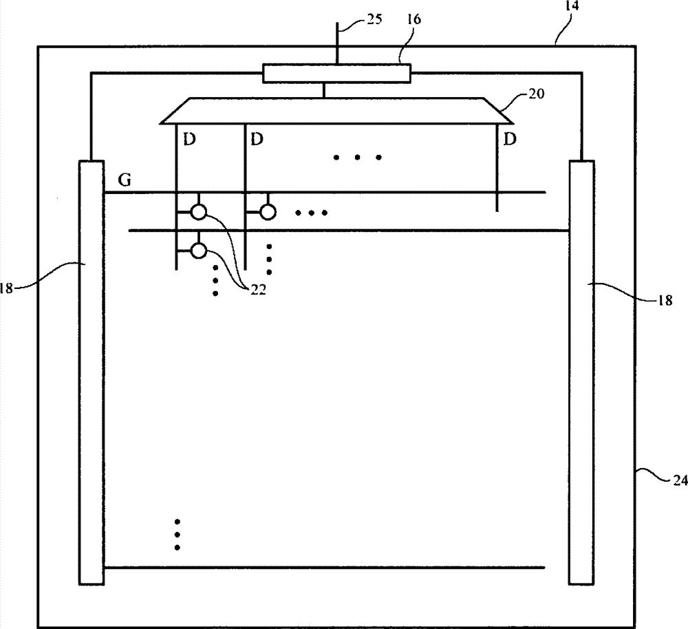
[0021] Displays in electronic devices may be provided with drive circuitry for displaying images on an array of pixels. figure 1 An example display is shown in . Such as figure 1 As shown, display 14 may have one or more layers such as substrate 24 . Layers such as substrate 24 may be formed from insulating materials such as glass, plastic, ceramic, and / or other dielectrics. Substrate 24 may be rectangular or may have other shapes. A rigid substrate material (eg, glass) or a flexible substrate material (eg, a flexible polymer sheet such as a layer of polyimide or other material) may be used to form the substrate 24 .

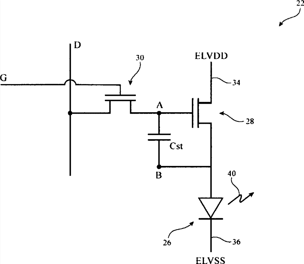
[0022] Display 14 may have an array of pixels 22 (sometimes referred to as a pixel circuit) for displaying images to a user. The array of pixels 22 may be formed from rows and columns of pixel structures on a substrate 24 . There may be any suitable number of rows and columns in the array of pixels 22 (eg, ten or more, one hundred or more, or one thousand o...


PUM


Abstract

The invention discloses an electronic equipment display device having pixel circuit arrays. Each pixel circuit can comprise organic light emitting diodes and driving transistors, each driving transistor can be adjusted to control the magnitude of a current flowing through the organic light emitting diodes, each pixel circuit can comprise a storage capacitor and one or more additional transistors such as switch transistors. Semiconductor oxide transistors and silicon transistors are used for forming pixel circuits. Storage capacitor and transistors can be formed through use of metal layers, semiconductor structures and dielectric layers. Some of the layers can be removed along the edge of a display device and therefore the display device can bend conveniently. The dielectric layers can have a multistep shape where data wires in the arrays are allowed to gradually lower toward the surface of a substrate when the data wires extend to an invalid edge area.

Description

[0001] This patent application claims priority to US Patent Application 14 / 494,931 filed September 24, 2014, which is hereby incorporated by reference in its entirety. Background technique [0002] The present invention relates generally to electronic devices, and more particularly to electronic devices with displays having thin film transistors. [0003] Electronic devices often include displays. For example, cellular telephones and portable computers include displays for presenting information to users. [0004] Displays such as organic light emitting diode displays have light emitting diode based pixel arrays. In this type of display, each pixel includes a light emitting diode and a thin film transistor that is used to control the application of signals to the light emitting diode. [0005] If care is not taken, the thin film transistor circuitry of a display can exhibit excessive transistor leakage current, insufficient transistor drive strength, poor area efficiency, hy...

Claims


Application Information

Patent Timeline
Patent Type & Authority Applications(China)
IPC IPC(8): H01L27/32
CPCY02E10/549H01L27/1251H01L27/1255H01L27/1225H10K59/1216H10K59/124H10K59/1213H10K59/131H10K77/111H10K2102/311H01L29/7869H01L29/78651H01L29/78672
Inventor 蔡宗廷V·格普塔林敬伟
Owner APPLE INC
Why Eureka
Try Eureka