Method for measuring stress optical coefficient of optical thin film

An optical coefficient, optical thin film technology, applied in the field of film stress optical coefficient measurement

Inactive Publication Date: 2015-02-18
THE 3RD ACAD 8358TH RES INST OF CASC
View PDF5 Cites 20 Cited by
  • Summary
  • Abstract
  • Description
  • Claims
  • Application Information

AI Technical Summary

Problems solved by technology
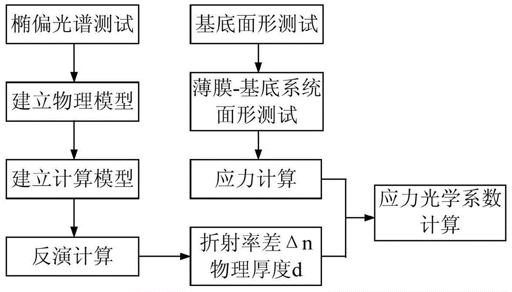
Thin films are generally thin solid layers with a thickness ranging from several monoatomic layers to several microns. The thin film material and the substrate form an interconnecte...

Method used


Image

  • Method for measuring stress optical coefficient of optical thin film
  • Method for measuring stress optical coefficient of optical thin film
  • Method for measuring stress optical coefficient of optical thin film

Examples


Embodiment 1

[0068] 1. Measuring method of stress optical constant of silicon dioxide film:

[0069] 1) Deposit silicon dioxide film by ion beam sputtering. The substrate material is a single-sided polished Φ25×1mm quartz wafer and an ultra-smooth surface Φ40×1mm silicon wafer. The surface roughness of the silicon wafer is less than 0.3nm, and the surface of the quartz wafer is The roughness is less than 1nm; the silicon wafer and the quartz wafer are completed under the same equipment and the same process parameters.

[0070] 2) Use a high-temperature test box to heat-treat the samples separately. The heat-treatment temperatures are 150°C, 250°C, 350°C, 450°C, 450°C, 550°C, and 650°C. The heat-treatment time is 24 hours, and the heating rate is 5°C / min. .

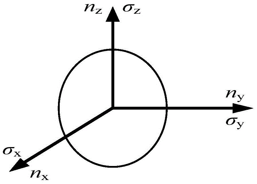
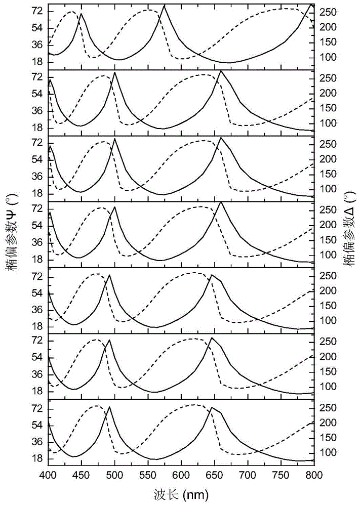
[0071] 3) Measure the reflection ellipsometric parameters Ψ(λ) and Δ(λ) of the silicon dioxide film with an ellipsometer, set the measurement wavelength range to 400nm-800nm, the measurement step size to 5nm, and the incident angle to...


PUM


Abstract

The invention belongs to the technical field of thin film stress optical coefficient measurement, and in particular relates to a method for measuring a stress optical coefficient of an optical thin film. The invention provides a method for measuring the stress optical coefficient of the thin film, especially for testing a stress optical constant of a silicon dioxide thin film material. The method is simple and convenient, so that research of a complicated optical test system is avoided; measurement on the stress optical coefficient of the silicon dioxide thin film material can be realized. particularly, stress and a birefringent characteristic of the thin film are measured, so that the stress optical coefficient of the thin film is calculated by a stress optical rule; the method is quick and convenient; the use of a complicated stress optical coefficient measurement system is avoided, and a new method and way are provided for the measurement of the stress optical coefficient of the thin film material.

Description

technical field [0001] The invention belongs to the technical field of thin film stress optical coefficient measurement, in particular to a method for measuring optical thin film stress optical coefficient. Background technique [0002] With the continuous expansion of applied optics, information optics, optical communication, optical imaging and optical detection technology, as well as the rapid development of computer technology, vacuum technology, and optoelectronic technology, thin-film optical components and thin-film electronic devices have been increasingly widely used. Since the preparation of optical thin films is completed in a strong non-equilibrium physical and chemical process, the stress of the thin film directly affects the stability and yield of thin-film optical components and thin-film electronic devices. When the film stress is high, film shedding such as curling and wrinkling occurs; when the film stress is small, film stress birefringence occurs, especia...

Claims


Application Information

Patent Timeline
IPC IPC(8): G01L1/24
Inventor 刘华松姜玉刚刘丹丹季一勤姜承慧王利栓杨霄
Owner THE 3RD ACAD 8358TH RES INST OF CASC
Why Eureka
Try Eureka