Heterojunction solar cell and manufacturing method thereof

A solar cell and heterojunction technology, which is applied in the field of solar cells, can solve the problems of large interface series resistance, improved filling factor of solar cells, disadvantages, etc.

Active Publication Date: 2015-02-18
ENN SOLAR ENERGY
View PDF4 Cites 6 Cited by
  • Summary
  • Abstract
  • Description
  • Claims
  • Application Information

AI Technical Summary

Problems solved by technology

[0008] An embodiment of the present invention provides a heterojunction solar cell and a manufacturing method thereof, which are used to solve the transmission barrier existing at the TCO / P-type amorphous silicon interface of the heterojunction solar cell structure existing in the prior art, so that the TCO / The interface series resistance of the P-type amorphous silicon interface is relatively large, which is not conducive to improving the fill factor of solar cells.

Method used


Image

  • Heterojunction solar cell and manufacturing method thereof
  • Heterojunction solar cell and manufacturing method thereof
  • Heterojunction solar cell and manufacturing method thereof

Examples


Embodiment Construction

[0037]In order to make the object, technical solution and advantages of the present invention clearer, the present invention will be further described in detail below in conjunction with the accompanying drawings. Obviously, the described embodiments are only some embodiments of the present invention, rather than all embodiments . Based on the embodiments of the present invention, all other embodiments obtained by persons of ordinary skill in the art without making creative efforts belong to the protection scope of the present invention.

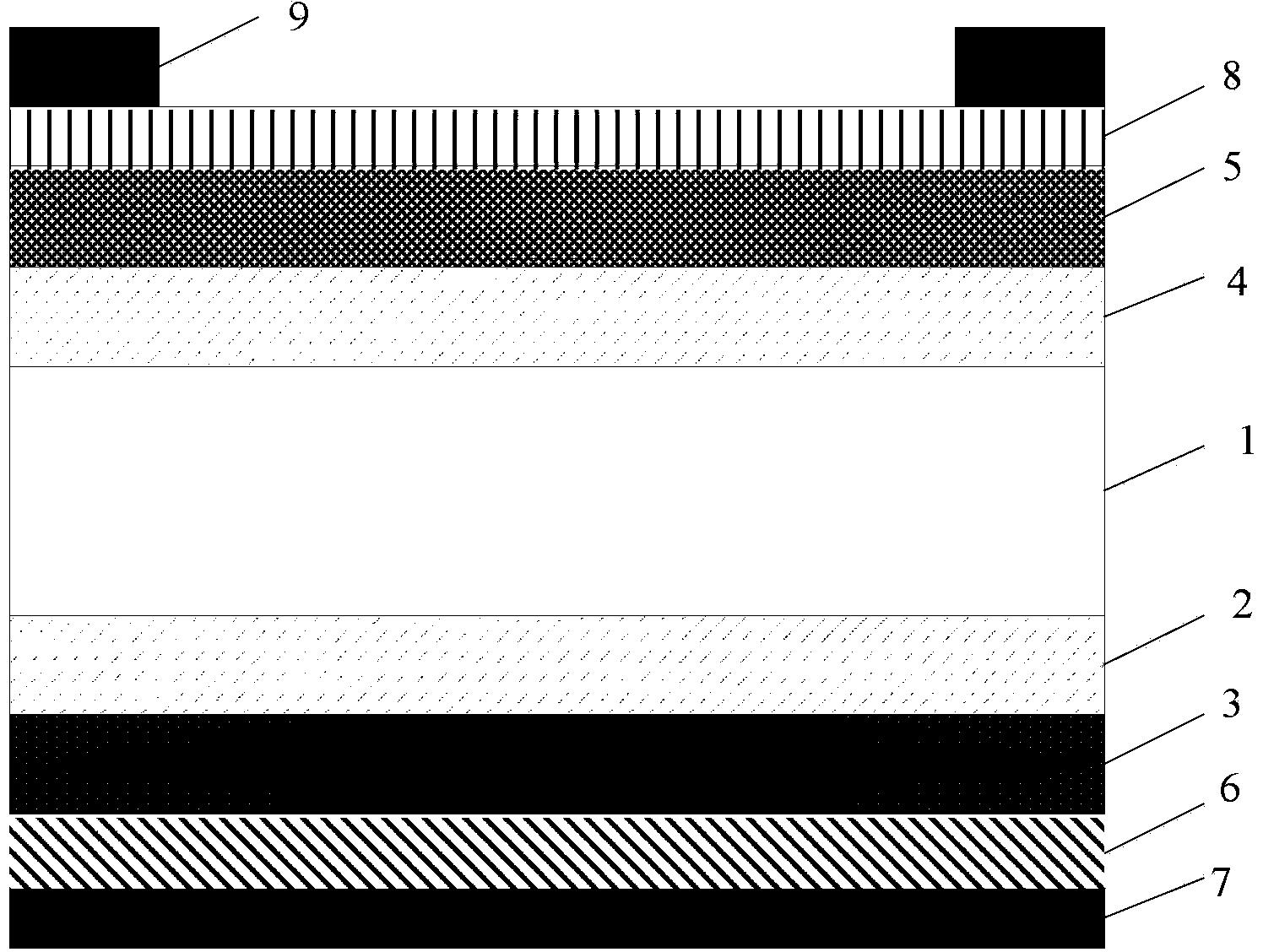
[0038] Such as figure 1 The illustrated structure schematic diagram of a heterojunction solar cell provided by the embodiment of the present invention, the solar cell includes:

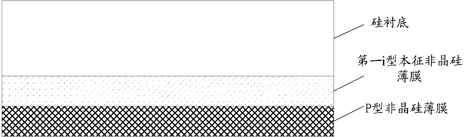
[0039] The first i-type intrinsic amorphous silicon film 2, the p-type amorphous silicon film 3 formed sequentially on the back side of the silicon substrate 1, the metal film 6 formed on the surface of the p-type amorphous silicon film 3, and the metal film 6 The...


PUM

PropertyMeasurementUnit
thicknessaaaaaaaaaa
thicknessaaaaaaaaaa
thicknessaaaaaaaaaa

Abstract

The invention discloses a heterojunction solar cell and a manufacturing method thereof. A metal film is formed on the surface of a p-type amorphous silicon film on a backlight face, and a back metal electrode is formed on the surface of the metal film. Since work function of the metal film is higher than that of the p-type amorphous silicon film, or a metallic compound is formed on an interface to form a barrier layer or a tunneling layer on the interface, the metal film/p-type amorphous silicon interface is in ohmic contact and pretty low in interface resistance, and compared with a traditional P-type amorphous silicon/TCO (transparent conductive oxide)interface structure, the metal film/p-type amorphous silicon interface has the advantages that high contact resistance between a TCO and the p-type amorphous silicon film is avoided while fill factor of the cell can be increased beneficially. In addition, due to the fact that the solar cell is in an inversion structure, light absorption of the metal film is avoided, and accordingly restriction on short-circuit current of the cell due to light absorption of the metal film is avoided.

Description

technical field [0001] The invention relates to the technical field of solar cells, in particular to a heterojunction solar cell and a manufacturing method thereof. Background technique [0002] As the cost ratio of solar cell BOS (Balance of System Components) increases, it becomes particularly important to improve cell conversion efficiency. The crystalline silicon heterojunction solar cell is considered to be the most competitive high-efficiency solar cell because of its low temperature preparation, low temperature coefficient and high conversion efficiency. [0003] The crystalline silicon heterojunction solar cell is composed of a variety of film layers, and there are various heterogeneous material interfaces between the various film layers, such as p-type amorphous silicon / TCO (Transparent Conductive Oxide, transparent conductive oxide), TCO / Ag and p-type amorphous silicon / i-type intrinsic amorphous silicon interfaces, these heterogeneous material interfaces affect t...

Claims


Application Information

Patent Timeline
Patent Type & Authority Applications(China)
IPC IPC(8): H01L31/0224H01L31/18
CPCH01L31/022425H01L31/18Y02E10/50Y02P70/50
Inventor 张林王进任明冲谷士斌何延如杨荣李立伟郭铁孟原
Owner ENN SOLAR ENERGY
Why Eureka
Try Eureka