A kind of LED electrode structure and manufacturing method thereof

A technology of electrode structure and manufacturing method, applied in circuits, electrical components, semiconductor devices, etc., can solve the problems of unstable electrochemical properties of Ag, sensitive preparation process, easy electrode falling off, etc., so as to improve external quantum efficiency and improve luminescence. Efficiency, reasonable structure design effect

Active Publication Date: 2017-02-08
XIANGNENG HUALEI OPTOELECTRONICS
View PDF5 Cites 0 Cited by
  • Summary
  • Abstract
  • Description
  • Claims
  • Application Information

AI Technical Summary

Problems solved by technology

[0003] At present, the traditional P and N electrodes generally adopt Ni / Au structure or Cr / Pt / Au structure. These two metal electrode structures have better stability, but a large part of the light emitted from the light-emitting area inside the chip will be absorbed by the electrodes. , thereby reducing the luminous efficiency of the LED
There are also reflective layers that use metal Ag or Al as the electrode. Ag has high reflectivity and can be directly deposited on p-GaN to form a good ohmic contact, but its adhesion is poor, and the electrochemical properties of Ag are unstable. , sensitive to the preparation process, easy to oxidize in the air, and will condense when exposed to high temperature
Al can form a strong and stable ohmic contact on n-GaN, but Al cannot form a good ohmic contact on p-GaN
In order to solve the problem of ohmic contact and adhesion, a thin film is usually designed between Al and GaN, but the thin film will absorb light, thus affecting the luminous efficiency of LED
[0004] Patent Application No. 200410058035.7 "Al / Ti / Aluminum / Nickel / Gold Ohmic Contact System for Gallium Nitride Devices" discloses an Al / Ti / Al / Ni / Au electrode, in which the Al layer directly Contact with the GaN surface can guarantee the luminous efficiency of the LED, but there are two problems: one is that the adhesion between the entire electrode and GaN will be poor, and the electrode is easy to fall off during the subsequent wire bonding and bonding process; the other is voltage will increase

Method used


Image

  • A kind of LED electrode structure and manufacturing method thereof
  • A kind of LED electrode structure and manufacturing method thereof

Examples


Embodiment 1

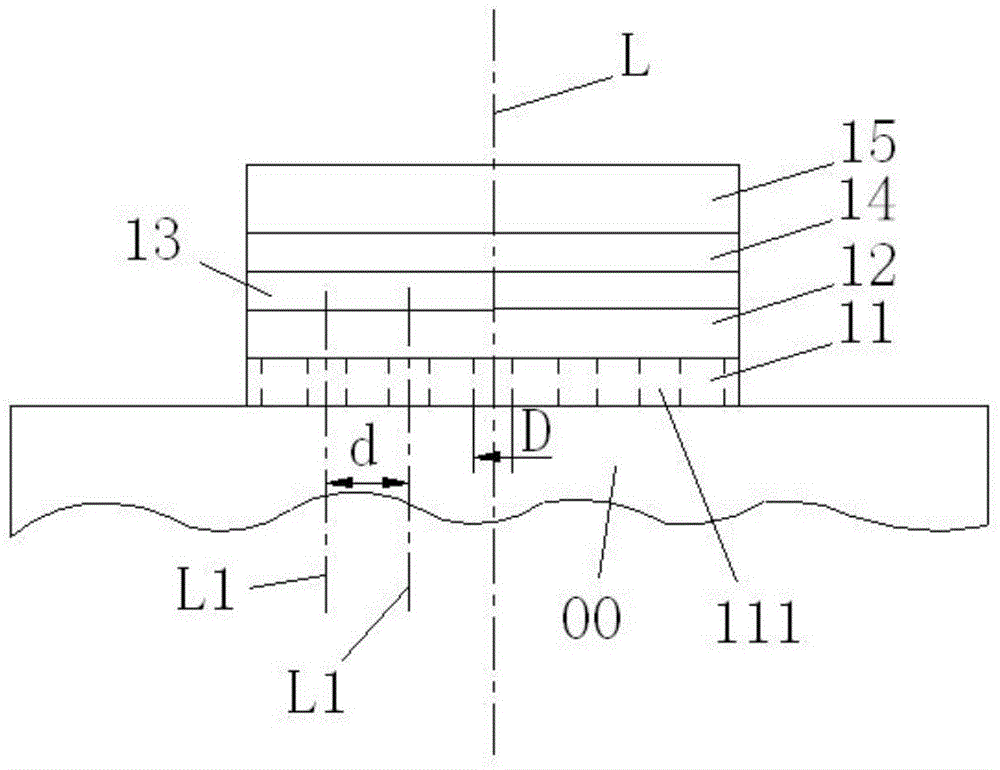
[0038] A LED electrode structure, see figure 1 , comprising a first Ni layer 11, an Al layer 12, a Cr layer 13, a second Ni layer 14 and an Au layer 15, the first Ni layer 11 is plated on the GaN layer 00 comprising n-GaN or / and p-GaN On the surface layer, the Al layer 12 is plated on the first Ni layer 11, the Cr layer 13 is plated on the Al layer 12, and the second Ni layer 14 is plated on the Cr layer 13, so The Au layer 15 is located on the outermost layer and plated on the second Ni layer 14 .

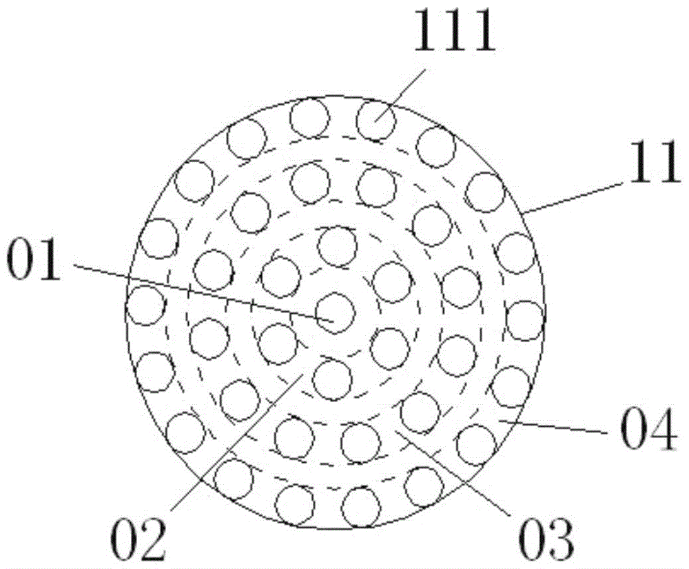
[0039] The first Ni layer 11 is provided with a through hole 111 along the central axis L of the LED electrode; on a plane perpendicular to the central axis L of the LED electrode, the cross section of the through hole 111 is circular; The number of through holes 111 is 37, which are uniformly arranged in the first row 01, the second row 02, the third row 03 and the fourth row 04 centered on the central axis L of the LED electrode from the inside to the outside. The number of th...


PUM


Abstract

The invention firstly aims to provide an LED electrode structure. A first Ni layer, an Al layer, a Cr layer, a second Ni layer and an Au layer are sequentially included from the surface layer of a GaN layer, and through holes are formed in the first Ni layer. The Al layer is designed to be closely next to the first Ni layer and can reflect the light transmitted to a P electrode and an N electrode to the inside of a chip, the reflected light is emitted out from the inside of the chip again, and therefore the external quantum efficiency of an LED chip is improved. Cr can achieve an adhesion effect and also can prevent Al metal atoms from diffusing towards the Ni layer and the Au layer above the electrodes, and the stability of the electrodes is improved. The design of the through holes can reduce the absorption to the light of the first Ni layer, the light-emitting efficiency is maximally improved, and the good contact of the Al layer and the surface of GaN can also be guaranteed. The invention secondarily aims to provide a manufacturing method of the LED electrode structure. The manufacturing method is simple, concise and suitable for mass production. The adhesivity between film layers is very good, and the stability of the entire electrode is good.

Description

technical field [0001] The invention relates to the field of optoelectronic devices, in particular to an LED electrode structure and a manufacturing method thereof. Background technique [0002] LED is a solid light source, which is a light-emitting device made of semiconductor P-N junction. During forward conduction, the minority carriers in the semiconductor recombine with the majority carriers, and the released energy is emitted in the form of photons or partly in the form of photons. Semiconductor LED lighting has significant advantages such as high efficiency, energy saving, environmental protection, long service life, etc., and has been widely used in various fields such as street lamps, display screens, indoor lighting, and automobile lights. How to improve luminous efficiency is the main problem that LED needs to solve. [0003] At present, the traditional P and N electrodes generally adopt Ni / Au structure or Cr / Pt / Au structure. These two metal electrode structures...

Claims


Application Information

Patent Timeline
Patent Type & Authority Patents(China)
IPC IPC(8): H01L33/40H01L33/38
CPCH01L33/38H01L33/405H01L2933/0016
Inventor 徐平王远红谈健夏晟
Owner XIANGNENG HUALEI OPTOELECTRONICS
Why Eureka
Try Eureka