
Method for improving shallow trench isolation edge sic stress performance

A shallow trench and stress technology, applied in electrical components, semiconductor/solid-state device manufacturing, circuits, etc., can solve the problems of low SiC growth, inability to provide enough, lack, etc., to improve process capability and enhance SiC epitaxial growth capability Effect

Active Publication Date: 2017-07-11
SHANGHAI HUALI MICROELECTRONICS CORP
View PDF5 Cites 0 Cited by
  • Summary
  • Abstract
  • Description
  • Claims
  • Application Information

AI Technical Summary

Problems solved by technology

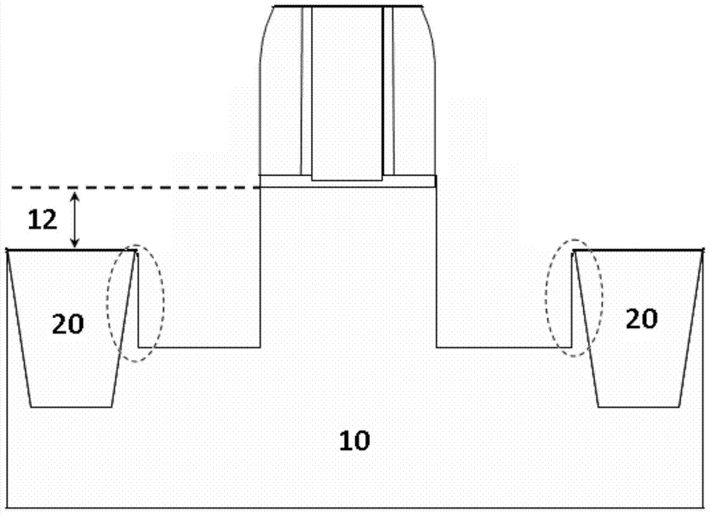
[0005] All of the above research and development are based on silicon substrates, that is to say, silicon substrates provide the seeds for SiC growth, and SiC grows epitaxially along the crystal lattice of silicon. However, in the semiconductor process, devices are separated by shallow trenches. The process (STI) achieves electrical isolation, and silicon dioxide is used for filling in STI. Therefore, at the edge of STI and the active area, the SiC epitaxial process will be affected by STI. STI cannot provide enough silicon "seeds", and SiC will appear. The SiC growth on the left and right sides of the STI edge in the selective epitaxy process is low or even absent

Method used

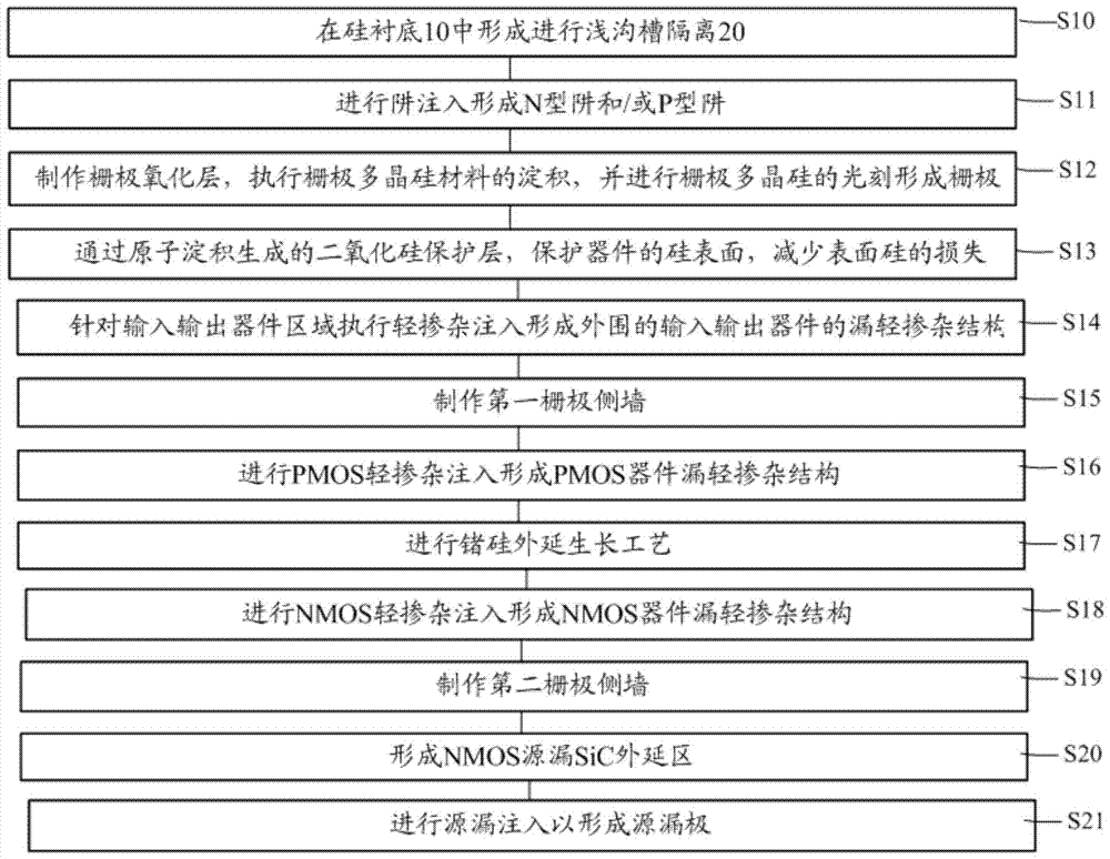

Image

  • Method for improving shallow trench isolation edge sic stress performance
  • Method for improving shallow trench isolation edge sic stress performance
  • Method for improving shallow trench isolation edge sic stress performance

Examples


Embodiment Construction

[0021] In order to make the content of the present invention clearer and easier to understand, the content of the present invention will be described in detail below in conjunction with specific embodiments and accompanying drawings.

[0022] Through research, the inventors advantageously found that the reason for the low or even missing SiC growth on the left and right sides of the STI edge is due to the height difference between the shallow trench isolation (STI) silicon oxide layer and the silicon surface of the active region. When the STI height is lower than On the surface of silicon AA in the active area of ​​the device, during the embedded silicon etching process, the silicon above the STI surface is etched away, which cannot provide silicon "seeds" for subsequent SiC growth, resulting in SiC on the left and right STI edges. Growth is reduced or even absent. Therefore, if figure 1 As shown, the height difference 12 between the STI silicon oxide layer 20 and the silico...


PUM


Abstract

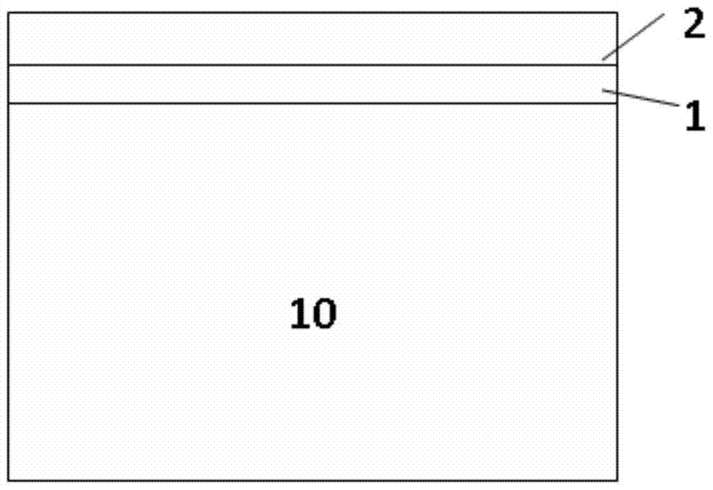
The invention provides a method for improving SiC stress property of a shallow trench isolation edge. The method comprises the steps of: firstly, depositing a silicon dioxide cushion layer with a first thickness and a silicon nitride cushion layer with a second thickness on the surface of a silicon substrate in sequence; secondly, with respect to the utilized photoetching process, choosing the first thickness of the silicon dioxide cushion layer to control a shallow trench isolation height to be formed, wherein the chosen silicon dioxide cushion layer satisfies the photoetching requirement and the stress requirement of the silicon nitride cushion layer with the second thickness; thirdly, actively photoetching and etching the silicon dioxide cushion layer, the silicon nitride cushion layer and the silicon substrate so as to form a groove in the silicon substrate; fourthly, filling silicon dioxide in the groove and flattening the filled silicon dioxide through chemical and mechanical grinding to form shallow trench isolation; peeling off the silicon nitride cushion layer and partially removing the silicon dioxide cushion layer to form the silicon dioxide cushion layer with the preset residual thickness.

Description

technical field [0001] The invention relates to the field of semiconductor manufacturing, and more specifically, the invention relates to a method for improving the stress performance of shallow trench isolation edge SiC by optimizing the Pad Oxide process. Background technique [0002] With the rapid development of VLSI technology, the size of MOSFET devices is continuously reduced, which usually includes the reduction of the channel length of MOSFET devices, the thinning of gate oxide layer thickness, etc. to obtain faster device speed. However, with the development of VLSI technology to the ultra-deep submicron level, especially when the technology node is 90 nanometers and below, reducing the channel length will bring a series of problems. In order to control the short channel effect, it will be in the channel Doping with a higher concentration of impurities will reduce the mobility of carriers, resulting in a decrease in device performance. It is difficult to simply red...

Claims


Application Information

Patent Timeline
Patent Type & Authority Patents(China)
IPC IPC(8): H01L21/336
CPCH01L21/76224H01L29/66553
Inventor 周建华
Owner SHANGHAI HUALI MICROELECTRONICS CORP
Learn More