Crystalline silicon solar cell wet chemical treatment method for performing texture surface making and cleaning steps
A solar cell and wet chemical treatment technology, which is applied to circuits, photovoltaic power generation, electrical components, etc., can solve problems such as the impact of cleaning effects, general anti-reflection effects, and reduced service life of cleaning liquids, so as to prevent cross-contamination of solutions and avoid unnecessary Uniform etching and improved productivity
- Summary
- Abstract
- Description
- Claims
- Application Information
AI Technical Summary
Problems solved by technology
Method used
Image

Examples
Embodiment 1
[0040] The operation of the velvet section is as follows:
[0041] (1) Provide a pre-treated silicon wafer; the pre-treatment is: put the silicon wafer in the flower basket into pure water to soak and overflow, rinse for 5 minutes, and remove dust, etc. The resistivity of pure water is 10-18MΩ.
[0042] (2) Pre-cleaning the silicon wafer with the first cleaning solution to remove particle impurities and pollution on the surface of the silicon wafer;
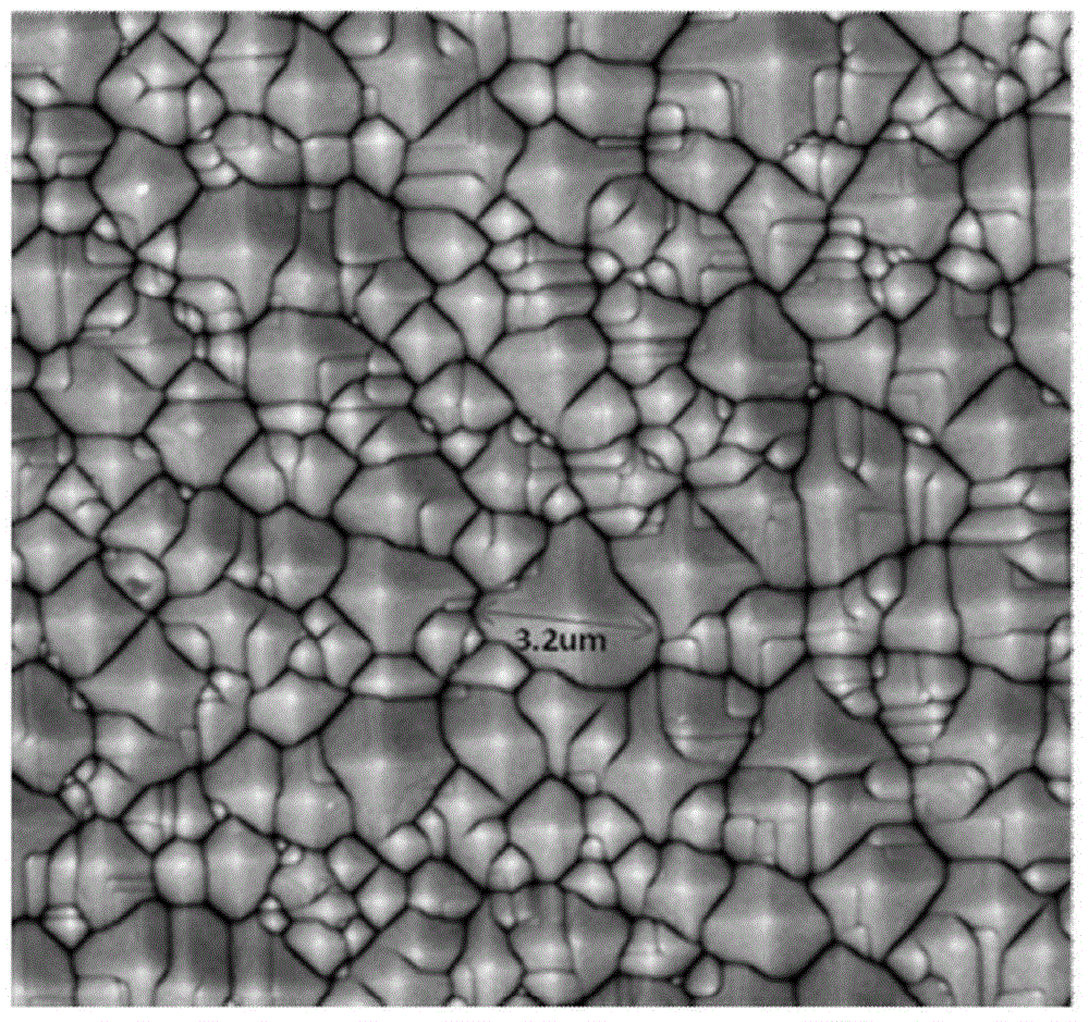
[0043] (3) The silicon wafer is polished with a polishing etchant to corrode the mechanically damaged layer on the surface. The mechanically damaged layer is as follows: image 3 shown;
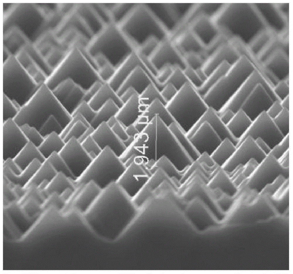
[0044] (4) adopt texturing liquid to carry out texturing process to silicon chip, make its surface form the textured structure;
[0045] (5) Using the second cleaning solution to clean the silicon wafer to remove surface metal ions, neutralize alkaline impurities, and reduce surface chemical residues;
[0046] (6) Treat the silicon wafer wit...
Embodiment 2
[0068] The operation of the velvet section is as follows:
[0069] (1) Provide a pre-treated silicon wafer; the pre-treatment is: put the silicon wafer in the flower basket into pure water to soak and overflow, rinse for 8 minutes, and remove dust, etc. The resistivity of pure water is 10-18MΩ.
[0070] (2) Pre-cleaning the silicon wafer with the first cleaning solution to remove particle impurities and pollution on the surface of the silicon wafer;
[0071] (3) The silicon wafer is polished with a polishing etchant to corrode the mechanically damaged layer on the surface. The mechanically damaged layer is as follows: image 3 shown;
[0072] (4) adopt texturing liquid to carry out texturing process to silicon chip, make its surface form the textured structure;
[0073] (5) Using the second cleaning solution to clean the silicon wafer to remove surface metal ions, neutralize alkaline impurities, and reduce surface chemical residues;
[0074] (6) Treat the silicon wafer wit...
Embodiment 3
[0096] The operation of the velvet section is as follows:
[0097] (1) Provide a pre-treated silicon wafer; the pre-treatment is: put the silicon wafer in the flower basket into pure water to soak and overflow, rinse for 1 min, and remove dust, etc. The resistivity of pure water is 10-18MΩ.
[0098] (2) Pre-cleaning the silicon wafer with the first cleaning solution to remove particle impurities and pollution on the surface of the silicon wafer;
[0099] (3) The silicon wafer is polished with a polishing etchant to corrode the mechanically damaged layer on the surface. The mechanically damaged layer is as follows: image 3 shown;
[0100] (4) adopt texturing liquid to carry out texturing process to silicon chip, make its surface form the textured structure;
[0101] (5) Using the second cleaning solution to clean the silicon wafer to remove surface metal ions, neutralize alkaline impurities, and reduce surface chemical residues;
[0102] (6) Treat the silicon wafer with an o...
PUM
| Property | Measurement | Unit |
|---|---|---|
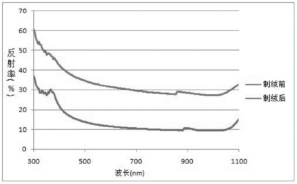
| reflectance | aaaaa | aaaaa |
Abstract
Description
Claims
Application Information
 - R&D
- Intellectual Property
- Life Sciences
- Materials
- Tech Scout
- Unparalleled Data Quality
- Higher Quality Content
- 60% Fewer Hallucinations
Browse by: Latest US Patents, China's latest patents, Technical Efficacy Thesaurus, Application Domain, Technology Topic, Popular Technical Reports.
© 2025 PatSnap. All rights reserved.Legal|Privacy policy|Modern Slavery Act Transparency Statement|Sitemap|About US| Contact US: help@patsnap.com