

Normally-closed high-electron-mobility transistor and manufacturing method thereof
A high electron mobility, normally closed technology, applied in semiconductor/solid-state device manufacturing, circuits, electrical components, etc., can solve the overall performance improvement of unsolved P-type layers, low on-resistance, and high electron mobility transistors and other problems to achieve the effect of protecting the surface quality, avoiding surface damage and optimizing the design
- Summary
- Abstract
- Description
- Claims
- Application Information
AI Technical Summary
Problems solved by technology
Method used
Image

Examples
Embodiment 1
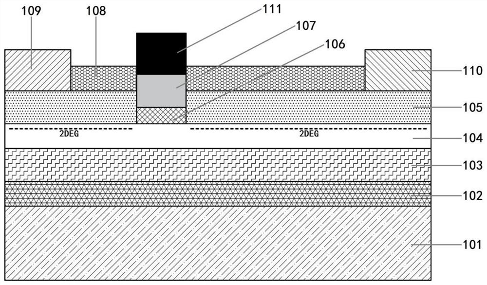
[0048] A method for manufacturing a normally-off AlGaN / GaN high electron mobility transistor, comprising the following steps:
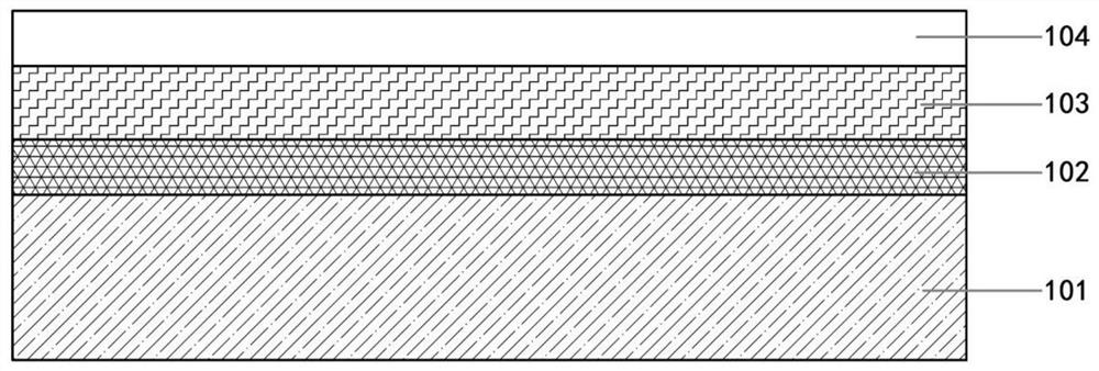
[0049] (1) if figure 2 As shown, a substrate 101 is provided, and a buffer layer 102, a high resistance layer 103 and a GaN channel layer 104 are sequentially grown on the substrate 101;
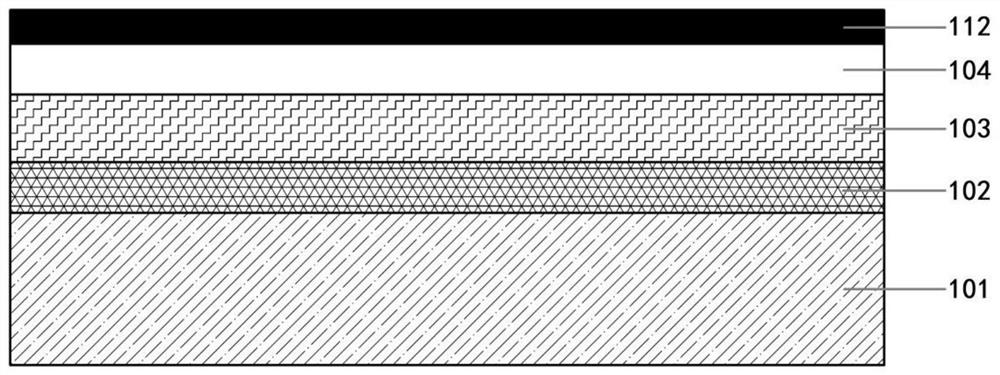
[0050] (2) if image 3 As shown, a first mask layer 112 is deposited on the GaN channel layer 104, and the first mask layer 112 is SiO 2 or SiN;
[0051] (3) if Figure 4 As shown, the first mask layer 112 that needs to grow the region outside the gate AlGaN layer 106 is etched away by photolithography etching technology;
[0052] (4) if Figure 5 As shown, using the first mask layer 112 to perform selective epitaxy, the AlGaN barrier layer 105 is grown on the GaN channel layer 104, and the first polycrystalline layer 113 is formed on the first mask layer 112;
[0053] (5) if Figure 6 As shown, the first polycrystalline layer 113 and the first mask layer 11...
PUM
| Property | Measurement | Unit |
|---|---|---|
| Thickness | aaaaa | aaaaa |
| Thickness | aaaaa | aaaaa |
| Thickness | aaaaa | aaaaa |
Abstract
Description
Claims
Application Information