
A normally-off high electron mobility transistor and its manufacturing method

A technology with high electron mobility and manufacturing methods, which is applied in semiconductor/solid-state device manufacturing, circuits, electrical components, etc., can solve problems such as unfavorable normally closed AlGaN/GaN, low on-resistance, and unresolved P-type layers. Achieve the effect of optimizing the two-dimensional electron gas concentration, avoiding surface damage, and protecting surface quality

Active Publication Date: 2022-06-21
JIANGSU UNIV
View PDF6 Cites 0 Cited by
  • Summary
  • Abstract
  • Description
  • Claims
  • Application Information

AI Technical Summary

Problems solved by technology

At the same time, this solution does not solve the problems caused by dry etching the P-type layer in the area outside the gate.
[0006] It can be seen that in the prior art, in order to increase the threshold voltage of the normally closed AlGaN / GaN high electron mobility transistor, other problems will be caused, which is not conducive to the improvement of the comprehensive performance of the normally closed AlGaN / GaN high electron mobility transistor
That is to say, performances such as high threshold voltage, threshold voltage consistency, low on-resistance, and high stability cannot be achieved at the same time.

Method used

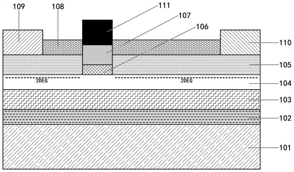

Image

  • A normally-off high electron mobility transistor and its manufacturing method
  • A normally-off high electron mobility transistor and its manufacturing method
  • A normally-off high electron mobility transistor and its manufacturing method

Examples


Embodiment 1

[0048] A method for manufacturing a normally-off AlGaN / GaN high electron mobility transistor, comprising the following steps:

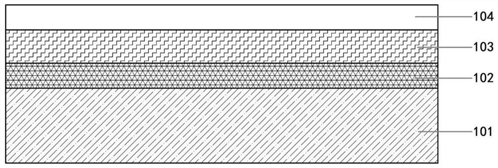
[0049] (1) If figure 2 As shown, a substrate 101 is provided, and a buffer layer 102, a high resistance layer 103 and a GaN channel layer 104 are grown on the substrate 101 in sequence;

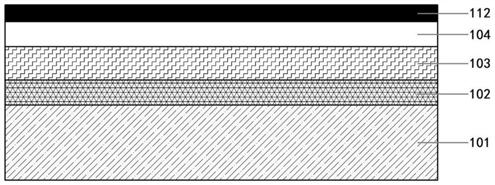
[0050] (2) If image 3 As shown, a first mask layer 112 is deposited on the GaN channel layer 104, and the first mask layer 112 is SiO 2 or SiN;

[0051] (3) If Figure 4 As shown, the first mask layer 112 that needs to grow the region outside the gate AlGaN layer 106 is etched away by using a photolithography etching technique;

[0052] (4) If Figure 5 As shown, the selective epitaxy is performed using the first mask layer 112, the AlGaN barrier layer 105 is grown on the GaN channel layer 104, and the first polycrystalline layer 113 is formed on the first mask layer 112 at the same time;

[0053] (5) If Image 6 As shown, the first polycrystalline layer 113...


PUM

PropertyMeasurementUnit
thicknessaaaaaaaaaa
thicknessaaaaaaaaaa
thicknessaaaaaaaaaa

Abstract

The invention belongs to the technical field of semiconductors, in particular to a normally-off high electron mobility transistor and a manufacturing method. In the present invention, the gate AlGaN layer and the P-type layer at the gate position, and the AlGaN barrier layer in the area outside the gate can be designed and grown independently by two selective epitaxy methods, and the composition and thickness can be precisely controlled. , so as to realize the optimal design of the threshold voltage, the two-dimensional electron gas concentration under the gate when it is turned on, and the two-dimensional electron gas concentration of the conductive channel outside the gate when it is turned on, without interfering with each other, and at the same time, there is no It involves dry etching, but replaces it with wet selective etching, which protects the surface quality of the transistor to the greatest extent and avoids the adverse consequences of dry etching. The normally-off AlGaN / GaN high electron mobility transistor obtained based on the manufacturing method of the present invention can have both high threshold voltage, consistency of threshold voltage, low on-resistance, and high stability.

Description

technical field [0001] The invention belongs to the technical field of semiconductors, and in particular relates to a normally-closed high electron mobility transistor and a manufacturing method. Background technique [0002] Compared with the first and second-generation semiconductor materials, the third-generation semiconductor GaN materials have the advantages of large band gap, high breakdown field strength, high electron mobility, and strong radiation resistance. GaN-based high electron mobility transistors are used in wireless High-frequency and high-power fields such as communication base stations, radar, and automotive electronics have great potential for development. The emergence of the AlGaN / GaN high electron mobility transistor (AlGaN / GaN HEMT) structure is based on the phenomenon described by T. Mimura et al. High electron mobility, commonly referred to as two-dimensional electron gas (2DEG). AlGaN / GaN high electron mobility transistors usually have two types:...

Claims


Application Information

Patent Timeline
Patent Type & Authority Patents(China)
IPC IPC(8): H01L29/778H01L21/335
CPCH01L29/7786H01L29/66462
Inventor 刘军林吕全江
Owner JIANGSU UNIV
Learn More