Rigid-flexible combined circuit board and manufacturing method thereof

A rigid-flexible combination and circuit board technology, which is applied in the manufacture of printed circuits, printed circuits, printed circuit components, etc., can solve the problems of difficulty in opening blind holes, achieve stable dimensions, good surface copper uniformity, and reduce difficulty Effect

Active Publication Date: 2015-03-04
GUANGZHOU FASTPRINT CIRCUIT TECH +2
View PDF3 Cites 27 Cited by
  • Summary
  • Abstract
  • Description
  • Claims
  • Application Information

AI Technical Summary

Problems solved by technology

[0006] Based on this, the purpose of the present invention is to overcome the defect that it is difficult to open blind holes on flexible substrates in the prior art, and to provide a method for preparing rigid-flexible circuit boards. Reduce the difficulty of opening blind holes, improve the accuracy and dimensional stability of blind holes

Method used


Image

  • Rigid-flexible combined circuit board and manufacturing method thereof
  • Rigid-flexible combined circuit board and manufacturing method thereof
  • Rigid-flexible combined circuit board and manufacturing method thereof

Examples


Embodiment

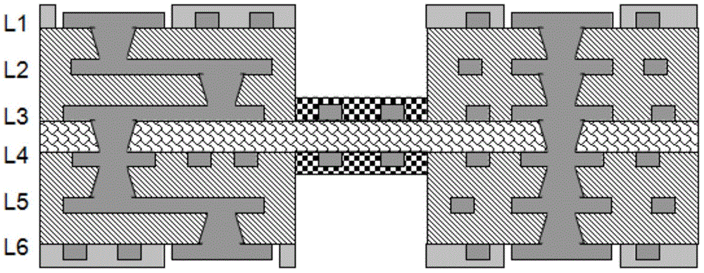
[0044] A rigid-flex circuit board with 6 layers in total, 3 / 4 of which are flexible layers, and the rest are rigid layers. The structure is as figure 1 Shown. The preparation method of the circuit board is as follows:

[0045] 1. Production of flexible core board.

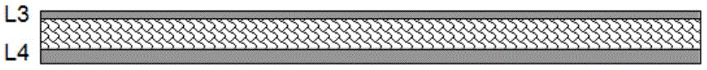
[0046] (1) Drilling: The flexible sheet is made into a copper-yin copper structure with different copper layer thicknesses on both sides in the form of single-sided thinned copper, such as figure 2 Shown, the two sides of the copper layer thickness are H1 and H2 flexible board. Among them, the copper thickness H1 on the L3 surface is 8-10μm, and the copper thickness H2 on the L4 surface is 18-70μm. It is understandable that the thickness of H1 and H2 can be set according to the design requirements, and only H1 is less than H2.

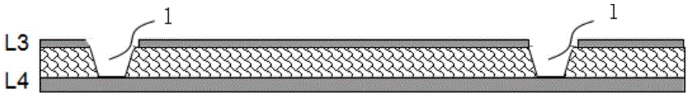
[0047] Before drilling, drill four positioning holes on the four corners of the flexible plate with a drill with a diameter of 3.175mm for the laser drilling machine to locate.

[0048] Use CO af...


PUM


Abstract

The invention discloses a rigid-flexible combined circuit board and a manufacturing method thereof and belongs to the technical field of printed circuit boards. The manufacturing method comprises the steps of manufacturing of flexible core boards, manufacturing of rigid core boards, manufacturing of rigid-flexible sub-boards and depth-controlling and groove-milling; the manufacturing step of the flexible core boards comprises the steps of: (1) drilling holes: choosing flexible boards with two copper layers having thicknesses of H1 and H2, in which H1 is less than H2); and drilling blind holes on the copper surface with the thickness of H1 by a laser drill; (2) plating holes; and (3) circuits; the manufacturing step of the rigid-flexible core boards comprises laminating the flexible core boards and the rigid core boards with non-flowing prepregs; the depth-controlling and groove-milling step comprises performing depth-controlling and groove-milling to open windows and expose the flexible zones. According to the rigid-flexible combined circuit board and the manufacturing method thereof, the difficulty of drilling blind holes on the flexible substrate is reduced to lay a foundation for realizing mass production of the rigid-flexible combined circuit boards. The rigid-flexible combined circuit board prepared by the method has the advantages of high accuracy and dimension stability of the blind holes, good uniformity of surface copper and good flexibility of flexible zones.

Description

Technical field [0001] The invention relates to the technical field of printed circuit boards, in particular to a rigid-flex circuit board and a preparation method thereof. Background technique [0002] With the development of electronic products in the direction of miniaturization and portability, the printed circuit boards they need are also developing in the direction of light, thin, short and small. Among them, the high-density interconnection (HDI) rigid-flex printed circuit board with high-density wiring and contacts and capable of three-dimensional assembly is the leader in line with this development direction. [0003] In recent years, the annual growth rate of HDI rigid-flex circuit board market demand has exceeded 20%, which is far greater than other types of printed circuit boards. The demand for HDI rigid-flex circuit board product structure has also evolved from the initial 1-level blind buried via structure to a high multi-level blind buried via structure. With the ...

Claims


Application Information

Patent Timeline
Patent Type & Authority Applications(China)
IPC IPC(8): H05K3/36H05K1/14
CPCH05K1/0298H05K3/4611H05K3/4626H05K2203/14
Inventor 林楚涛莫欣满陈蓓
Owner GUANGZHOU FASTPRINT CIRCUIT TECH
Why Eureka
Try Eureka