Graphite bearing disc used for production process of LED epitaxial wafer

A carrier plate and epitaxy technology, which is used in the manufacture of semiconductor/solid-state devices, electrical components, and electrical solid-state devices, etc., can solve the problems of uneven brightness of epitaxial wafers, low luminous intensity, and increased non-radiative composite luminescence, so as to improve luminescence. The effect of low intensity, reduced eddy current area, and improved brightness uniformity

Active Publication Date: 2015-03-11
XIAMEN SANAN OPTOELECTRONICS TECH CO LTD
View PDF5 Cites 29 Cited by
  • Summary
  • Abstract
  • Description
  • Claims
  • Application Information

AI Technical Summary

Problems solved by technology

Using a traditional MOCVD reaction chamber to grow LED epitaxial wafers, such as figure 2 As shown, because the high-speed rotating airflow sprayed downward from the top cover will generate a certain thermal buoyancy convection at the center of the graphite carrier plate, forming a vortex 102 in a local area, causing the inner ring of the epitaxial wafer (with the flat side of the substrate facing the carrier) Take the center of the disk as an example) the dislocation density of tiny Pits in the area of ​​about 0-20 mm near the flat edge increases, and the half-width of the XRD (002) plane and XRD (102) plane is larger than the central area of ​​the epitaxial wafer, causing the local The non-radiative recombination luminescence in the area becomes larger, and the luminous intensity is low (down about 40~60%), which leads to the uneven brightness of the epitaxial wafers in the inner circle.

Method used


Image

  • Graphite bearing disc used for production process of LED epitaxial wafer
  • Graphite bearing disc used for production process of LED epitaxial wafer
  • Graphite bearing disc used for production process of LED epitaxial wafer

Examples


Embodiment 1

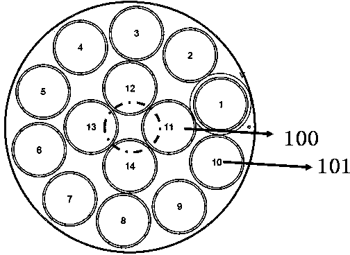
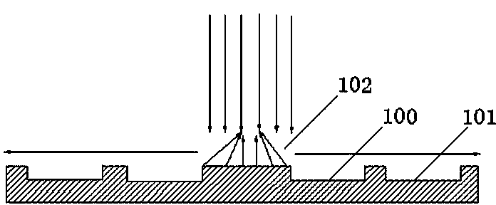
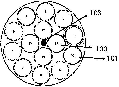
[0033] refer to Figure 3~Figure 4 As shown, a graphite carrier plate for LED epitaxial wafer manufacturing process includes: 14 4-inch wafer grooves arranged above the carrier plate, 4 wafer grooves 100 are distributed on the inner ring, and 10 wafer grooves are distributed on the outer ring The wafer groove 101 is used to place an epitaxial wafer substrate (not shown in the figure), wherein a convex structure 103 is provided in the center of the carrier plate, the center of which is high and the edge is low, serving as a flow guide layer for The vortex 102 at the center of the improvement.

[0034] In order to improve the vortex 102 at the center sufficiently and evenly, it is preferable that the protrusion structure is axisymmetric along the center of the carrier plate. In this embodiment, the shape of the protrusion structure is preferably hemispherical.

[0035] The material of the convex portion structure can be selected from graphite, silicon carbide, titanium metal, t...

Embodiment 2

[0039] refer to Figure 10 As shown, the difference from Example 1 is that the protrusion structure of this embodiment is curved, and the material of the protrusion structure is silicon carbide, which is formed on the central area of ​​the carrier plate by bonding, thereby changing the central setting The gas flow rate and direction can be reduced to reduce the probability and area of ​​thermal buoyancy convection, that is, eddy current, and improve the problem of low luminous intensity in the local area where the epitaxial wafer in the inner ring is facing the center of the carrier disk axis, thereby improving the uniformity of luminous intensity in the inner ring. Improve the overall brightness uniformity of the inner and outer ring epitaxial wafers.

Embodiment 3

[0041] refer to Figure 11As shown, different from Example 1, the convex structure of this example is triangular pyramid-shaped, as a guide layer, thereby changing the gas flow rate and direction arranged in the center, reducing the generation probability and area of ​​thermal buoyancy convection, that is, eddy current, Improve the problem of low luminous intensity in the local area where the epitaxial wafers in the inner ring are facing the center of the carrier disk axis, thereby improving the uniformity of the luminous intensity of the inner ring and improving the overall uniformity of brightness of the epitaxial wafers in the inner and outer rings.


PUM


Abstract

The invention discloses a graphite bearing disc used for a production process of an LED epitaxial wafer. The graphite bearing disc comprises a plurality of wafer grooves formed in the bearing disc, wherein the wafer grooves are used for containing epitaxial wafer substrates. The graphite bearing disc is characterized in that a convex part structure is arranged on a central region of the bearing disc so that the vortex area of the central region of the bearing disc in an epitaxial production process can be reduced, and the problem that the light intensity of a partial region, which is formed towards the center of a shaft of the bearing disc, of the epitaxial wafer of an inner ring is low can be solved; and therefore, the brightness uniformity of the inner ring is improved and the whole uniformity of the brightness of the epitaxial wafers of the inner and outer rings is improved.

Description

technical field [0001] The invention belongs to the technical field of semiconductors, and in particular relates to a graphite carrier plate used in an LED epitaxial wafer manufacturing process. Background technique [0002] Light Emitting Diode (English for Light Emitting Diode, referred to as LED) is a solid-state semiconductor diode light-emitting device, which is widely used in lighting fields such as indicator lights and display screens. [0003] At present, LED epitaxial wafers (or epitaxial wafers) are generally obtained by Metal-organic Chemical Vapor Deposition (Metal-organic Chemical Vapor Deposition, MOCVD in English), and the process is generally: the epitaxial wafer substrate (such as sapphire Substrate) is put into the groove of the graphite carrier (Wafer carrier in English), and together with the graphite carrier, it is introduced into the MOCVD reaction chamber. Organometallic compounds and III-V gases are repolymerized on the wafer substrate after pyrolys...

Claims


Application Information

Patent Timeline
Patent Type & Authority Applications(China)
IPC IPC(8): H01L21/673
CPCH01L21/673H01L21/67386H01L2221/67
Inventor 郑锦坚寻飞林邓和清李志明杜伟华伍明跃周启伦林峰李水清康俊勇
Owner XIAMEN SANAN OPTOELECTRONICS TECH CO LTD
Why Eureka
Try Eureka