

Light-emitting device and manufacturing method thereof
A light-emitting device and light technology, which is applied in the direction of organic light-emitting devices, organic light-emitting device structures, semiconductor/solid-state device manufacturing, etc., can solve the problems of high price, unfavorable large-scale production, complicated process, etc. The effect of large-scale production and simple process
- Summary
- Abstract
- Description
- Claims
- Application Information
AI Technical Summary
Problems solved by technology
Method used
Image

Examples
Embodiment Construction
[0030] In order to make the above objects, features and advantages of the present invention more comprehensible, specific implementations of the present invention will be described in detail below in conjunction with the accompanying drawings. In the following description, numerous specific details are set forth in order to provide a thorough understanding of the present invention. However, the present invention can be implemented in many other ways different from those described here, and those skilled in the art can make similar improvements without departing from the connotation of the present invention, so the present invention is not limited by the specific implementations disclosed below.
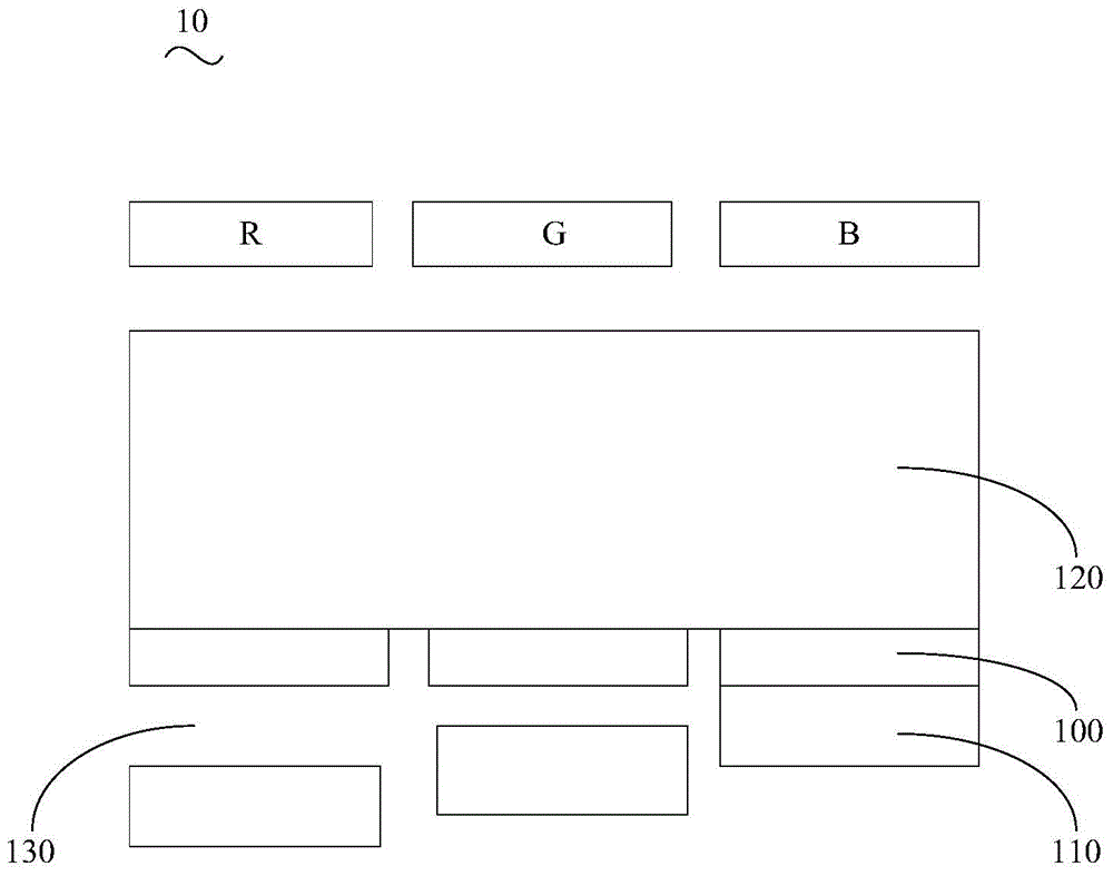
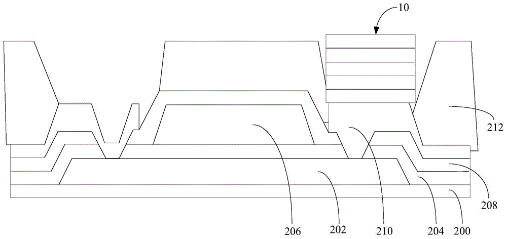
[0031] In a top emission type organic light emitting device, an upper electrode and a reflective layer disposed under a lower electrode function as a mirror so that light emitted from a light emitting layer of the organic light emitting device is reflected by the mirror. Therefore, de...
PUM
 Abstract
Description
Claims
Application Information