Manufacturing method of fine circuit of printed-circuit board

A technology for printed circuit boards and fine lines, applied in the fields of printed circuit manufacturing, printed circuits, electrical components, etc. Line grooves and other problems, to achieve the effect of regular shape, line width matching, and low cost

Inactive Publication Date: 2015-03-11
UNIV OF ELECTRONICS SCI & TECH OF CHINA
View PDF5 Cites 22 Cited by
  • Summary
  • Abstract
  • Description
  • Claims
  • Application Information

AI Technical Summary

Problems solved by technology

This method is to ablate the circuit groove on the substrate, and then make the circuit in the groove. This method can effectively avoid the problem of side erosion of the circuit, but due to the difference in the material of the substrate surf...

Method used


Image

  • Manufacturing method of fine circuit of printed-circuit board
  • Manufacturing method of fine circuit of printed-circuit board
  • Manufacturing method of fine circuit of printed-circuit board

Examples


Embodiment

[0031] A method for manufacturing fine lines of a printed circuit board, comprising the following steps:

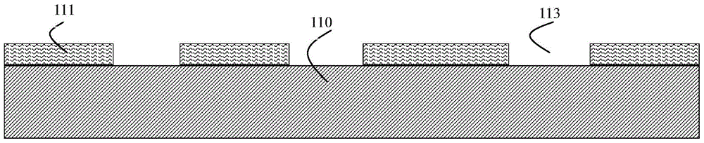
[0032] Step 1: paste the first dry film 111 on the surface of the copper-free substrate 110, and then perform exposure and development to obtain fine circuit grooves 113, such as figure 1 shown;

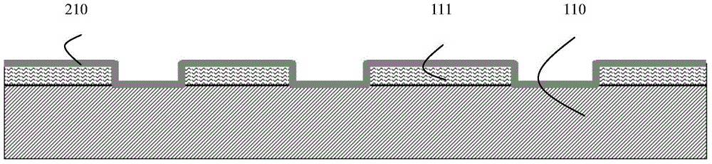
[0033] Step 2: Copper plating is performed on the surface of the base material treated in step 1, so that the upper surface of the first dry film 111 and the inner surface of the fine line groove 113 form a copper seed layer 210, such as figure 2 shown;

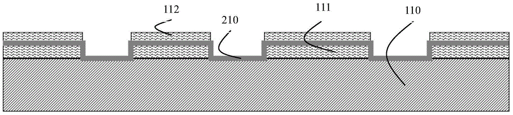
[0034] Step 3: Paste the second dry film 112 on the surface of the copper seed layer obtained after the treatment in step 2, and then perform exposure and development treatments to expose the fine line groove 113, such as image 3 shown;

[0035] Step 4: Carry out electroplating and copper filling treatment on the base material treated in step 3, and fill the fine line groove 113, such as Figure 4 shown;

[0036] Step 5:...


PUM

PropertyMeasurementUnit
Thicknessaaaaaaaaaa
Thicknessaaaaaaaaaa
Thicknessaaaaaaaaaa

Abstract

The invention provides a manufacturing method of a fine circuit of a printed-circuit board, and belongs to the field of the manufacture of the printed-circuit board. The method comprises the steps of forming a fine line slot by dry film pasting and exposure and development, and obtaining the fine line by carrying out deposition on a copper seed layer, dry film pasting, electroplating and copper filling, defilming, quick etching and the like. According to the method provided by the invention, the line width and line spacing of the circuit can be greatly reduced, and the lateral erosion problem generated when the copper seed layer is removed can be effectively prevented. The method provided by the invention is convenient to operate and low in cost, and expensive and complicate equipments can be prevented; furthermore, the slot of the fine line formed by the method is regular in shape, the problem that the shape of the slot formed by laser ablation is irregular can be overcome to obtain a complete line shape, and the shape of the line is matched with the designed line width to meet an impedance requirement.

Description

technical field [0001] The invention belongs to the field of printed circuit board manufacture, and in particular relates to a method for manufacturing fine lines of a printed circuit board. Background technique [0002] With the miniaturization of electronic equipment, the volume of electronic components is getting smaller and higher, and the arrangement density is getting higher and higher, which requires the circuit board as the carrier of electronic components to have smaller line width and line spacing; at the same time, the transmission of high-frequency signals and The requirements for the integrity of the transmission signal put forward higher requirements for the line impedance design of the circuit board, and the corresponding line pattern should have smaller side erosion, fewer defects, and better integrity. [0003] At present, there are mainly three methods for making fine circuits on circuit boards: subtractive method, semi-additive method, and full-additive me...

Claims


Application Information

Patent Timeline
IPC IPC(8): H05K3/20H05K3/10
CPCH05K3/107H05K2203/0502H05K2203/0789
Inventor 何为李松松何雪梅王守绪周国云陈苑明冀林仙
Owner UNIV OF ELECTRONICS SCI & TECH OF CHINA
Why Eureka
Try Eureka