Semiconductor package comprising ferrite antenna for near filed communication and manufacturing method thereof

A near-field communication and semiconductor technology, which is applied in semiconductor/solid-state device manufacturing, semiconductor devices, semiconductor/solid-state device components, etc., can solve problems such as poor molding of memory cards, shorten the manufacturing process time, improve antenna performance, and suppress Effects of Electromagnetic Interference

Inactive Publication Date: 2015-03-18
BARUN ELECTRONICS CO LTD
View PDF8 Cites 8 Cited by
  • Summary
  • Abstract
  • Description
  • Claims
  • Application Information

AI Technical Summary

Problems solved by technology

[0011] However, the molding process of the memory card is carried out under high temperature and high pressure conditions, so the air layer that is not filled with the liquid molding resin will expand under the high temperature and high pressure, which may cause poor molding of the memory card

Method used


Image

  • Semiconductor package comprising ferrite antenna for near filed communication and manufacturing method thereof
  • Semiconductor package comprising ferrite antenna for near filed communication and manufacturing method thereof
  • Semiconductor package comprising ferrite antenna for near filed communication and manufacturing method thereof

Examples


no. 1 Embodiment

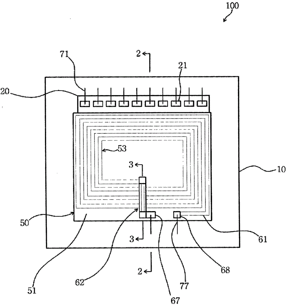
[0072] figure 1 It is a plan view showing a semiconductor package equipped with a ferrite antenna for near field communication according to the first embodiment of the present invention. figure 2 Yes figure 1 2-2 line profile. in addition, image 3 Yes figure 1 3-3 line profile.

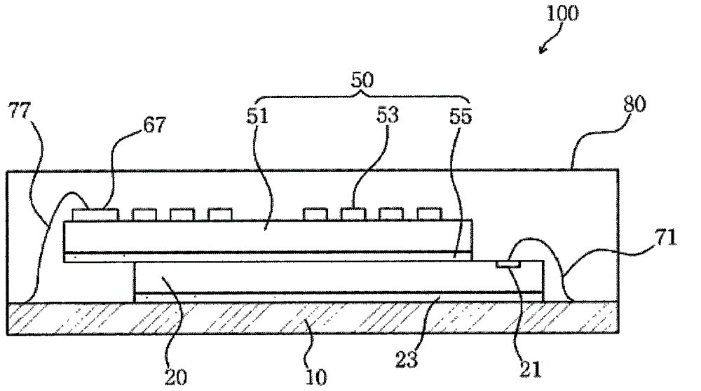
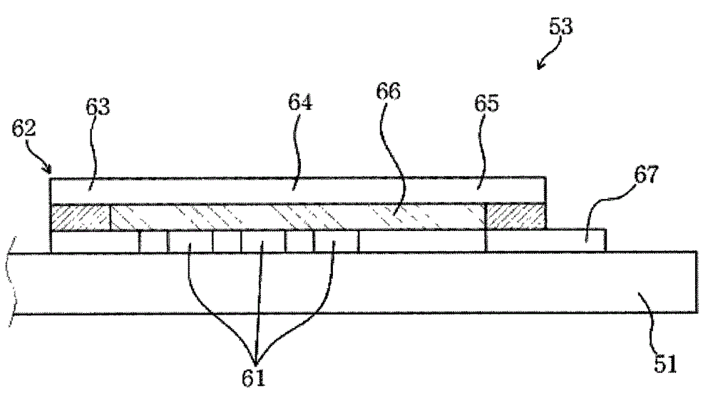
[0073] refer to Figure 1 to Figure 3 The semiconductor package 100 in the first embodiment includes a printed circuit board 10 , a semiconductor chip 20 , a ferrite antenna 50 for near field communication, a first bonding wire 71 , a second bonding wire 77 , and a resin seam portion 80 . The semiconductor chip 20 is mounted on the upper surface of the printed circuit board 10 . The ferrite antenna 50 is mounted on the semiconductor chip 20 , and includes a ferrite substrate 51 of ferrite material whose bottom surface is mounted on the semiconductor chip 20 , and an antenna radiation pattern 53 formed on the ferrite substrate 51 . The first bonding wire 71 electrically connects the semiconduc...

no. 2 Embodiment

[0113] Figure 9It is a cross-sectional view showing a semiconductor package 200 according to a second embodiment of the present invention.

[0114] refer to Figure 9 The semiconductor package 200 of the second embodiment has a structure in which a plurality of semiconductor chips 30 , 40 are laminated on the printed circuit board 10 , and a ferrite antenna 50 is laminated on the uppermost semiconductor chip 40 .

[0115] At this time, the plurality of semiconductor chips 30 and 40 include a first semiconductor chip 30 mounted on the upper surface of the printed circuit board 10 and a second semiconductor chip 40 laminated on the upper surface of the first semiconductor chip. When the second semiconductor chip 40 is laminated on the first semiconductor chip 30 , the first die pad 31 of the first semiconductor chip 30 is mounted so as to be exposed to the outside. In addition, when the ferrite antenna 50 is laminated on the upper surface of the second semiconductor chip 40, ...

no. 3 Embodiment

[0122] Figure 10 It is a cross-sectional view showing a semiconductor package 300 according to a third embodiment of the present invention.

[0123] refer to Figure 10 The semiconductor package 300 of the third embodiment has a structure in which the first semiconductor chip 30 and the second semiconductor chip 40 are laminated on the upper surface of the printed circuit board 10 , and the ferrite antenna 50 is laminated on the upper surface of the second semiconductor chip 40 .

[0124] In the semiconductor package 100 of the third embodiment, the first semiconductor chip 30, the second semiconductor chip 40, and the ferrite antenna 50 are laminated on the printed circuit board so that the first die pad 31 and the second die pad 41 are exposed to the outside. The structure on the circuit board is the same as that of the semiconductor package in the second embodiment ( Figure 9 200) is similar.

[0125] However, the semiconductor package 300 of the third embodiment is di...


PUM


Abstract

The present invention relates to a semiconductor package having a ferrite antenna for a near field communication (NFC), and a method of manufacturing the same. A semiconductor package according to the present invention includes a printed circuit board, a semiconductor chip, a ferrite antenna for NFC, first and second bonding wires, and a resin sealing part. The semiconductor chip is attached to one surface of the printed circuit board. The ferrite antenna, which is attached onto the semiconductor chip, includes a ferrite substrate of a ferrite material having the low surface attached onto the semiconductor chip, and an antenna pattern formed on the top surface of the ferrite substrate. The first wire connects the semiconductor chip and the printed circuit board electrically to each other. The second wire connects the antenna pattern of the ferrite antenna and the printed circuit board electrically to each other. And, the resin sealing part seals the semiconductor chip, the ferrite antenna, and the first and second bonding wires formed on the printed circuit board.

Description

technical field [0001] The invention relates to a semiconductor package, in particular to a semiconductor package equipped with a ferrite antenna in the package and capable of near field communication (near field communication; NFC) and a manufacturing method thereof. Background technique [0002] Semiconductor components that can be used in mobile communication terminals, PDA (Personal Data Assistant), PC (Personal Computer), smart phone (smart phone), tablet PC (tablet PC), etc., such as memory card (memory card) have various specifications. For example, MMC (Multi Media Card), HSMMC (High Speed ​​Multi Media Card), RSMMC (Reduced Size Multi Media Card), SD (Secure Digital) card, memory stick, memory stick pro and many other products. The bit rate, protocol for identifying the card, method of controlling the bus, data formatting, etc. are different for each memory card. [0003] In addition to the simple data storage function of these memory cards, the near field communic...

Claims


Application Information

Patent Timeline
Patent Type & Authority Applications(China)
IPC IPC(8): H01L23/498H01L23/31H01L21/60H01L21/56
CPCH01L2224/32145H01L2224/32225H01L2224/48091H01L2224/48227H01L2224/73265H01L2224/92247H01L2225/06562H01L2924/00014H01L2924/00H01L23/12
Inventor 金承炫姜义硕
Owner BARUN ELECTRONICS CO LTD
Why Eureka
Try Eureka