GOA circuit of low-temperature polycrystalline silicon thin film transistor

A technology of thin-film transistors and low-temperature polysilicon, which can be used in instruments, static indicators, etc., and can solve problems such as high power consumption and poor stability

Active Publication Date: 2015-03-25
SHENZHEN CHINA STAR OPTOELECTRONICS TECH CO LTD
View PDF5 Cites 21 Cited by
  • Summary
  • Abstract
  • Description
  • Claims
  • Application Information

AI Technical Summary

Problems solved by technology

[0006] The purpose of the present invention is to provide a low-temperature polysilicon semiconductor thin film transistor GOA circuit, which can solve the problem of poor stability and high power consumption of the device circuit of the LTPS single-type TFT; solve the problem of TFT leakage of the current single-type GOA circuit, optimize The performance of the circuit; and the design of ultra-narrow bezel or no bezel can be realized

Method used


Image

  • GOA circuit of low-temperature polycrystalline silicon thin film transistor
  • GOA circuit of low-temperature polycrystalline silicon thin film transistor
  • GOA circuit of low-temperature polycrystalline silicon thin film transistor

Examples


Embodiment Construction

[0077] In order to further illustrate the technical means adopted by the present invention and its effects, the following describes in detail in conjunction with preferred embodiments of the present invention and accompanying drawings.

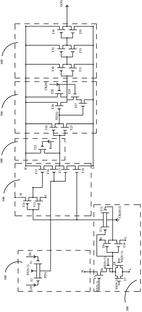
[0078] see figure 1 , is the circuit diagram of the first embodiment of the present invention. Such as figure 1 As shown, the present invention provides a low-temperature polysilicon thin film transistor GOA circuit for forward scanning transmission, including a plurality of GOA units cascaded, where N is a positive integer, and the Nth-level GOA unit adopts a plurality of N-type transistors and A plurality of P-type transistors, the Nth-level GOA unit includes: a transmission part 100, a transmission control part 200, a data storage part 300, a data clearing part 400, an output control part 500 and an output buffer part 600;

[0079]The transmission part 100 is electrically connected to the first low-frequency signal UD, the second low-freq...


PUM


Abstract

The invention provides a GOA circuit of a low-temperature polycrystalline silicon thin film transistor. The GOA circuit is used for forward scan transmission and comprises a plurality of cascaded GOA units, N is set to be a positive integer, a plurality of N-type transistors and a plurality of P-type transistors are adopted in the N class GOA unit, and the N class GOA unit comprises a transmission part (100), a transmission control part (200), a data storage part (300), a data clearing part (400), an output control part (500) and an output buffering part (600). Signals are transmitted between the upper and lower levels through a transmission gate, converted through an NOR gate logical unit and an NAND gate logical unit and stored and transmitted through a timing sequence phase inverter and a phase inverter, the problems that an LTPS single type TFT device is poor in circuit stability and large in power consumption, and the single type GOA circuit TFT leaks electricity are solved, the performance of the circuit is optimized, and the ultra-narrow frame or frameless design can be achieved.

Description

technical field [0001] The invention relates to the field of display technology, in particular to a low-temperature polysilicon thin film transistor GOA circuit. Background technique [0002] GOA (Gate Drive On Array), is to use thin film transistor (thin film transistor, TFT) liquid crystal display array (Array) manufacturing process to make the gate driver on the thin film transistor array substrate, so as to realize the driving method of progressive scanning. [0003] Usually, the GOA circuit is mainly composed of a pull-up part, a pull-up control part, a transfer part, a pull-down part, and a pull-down maintenance circuit part ( Pull-down Holding part) and the rising part (Boost part) which is responsible for raising the potential. The rising part is generally composed of a bootstrap capacitor. [0004] The pull-up part is mainly responsible for outputting the input clock signal (Clock) to the gate of the thin film transistor as a driving signal of the liquid crystal di...

Claims


Application Information

Patent Timeline
Patent Type & Authority Applications(China)
IPC IPC(8): G09G3/36
CPCG09G3/3677G09G2300/0408G09G3/36G09G2300/0417G09G2310/0243G09G2310/0286G09G2300/0814G09G2300/0819G09G2300/0871G09G2320/0214
Inventor 肖军城
Owner SHENZHEN CHINA STAR OPTOELECTRONICS TECH CO LTD
Why Eureka
Try Eureka