
Fan-out type packaging structure based on multiple layers of chips of organic substrate and packaging method

A multi-layer chip and packaging structure technology, applied in photovoltaic power generation, electrical components, climate sustainability, etc., can solve the problems of difficulty in applying large-scale mass production requirements, small application range, and low processing cost, and achieve improved heat dissipation Performance and electromagnetic shielding performance, wide application range, low CTE effect

Active Publication Date: 2015-03-25
NAT CENT FOR ADVANCED PACKAGING
View PDF4 Cites 3 Cited by
  • Summary
  • Abstract
  • Description
  • Claims
  • Application Information

AI Technical Summary

Problems solved by technology

[0002] The current fan-out packaging technology is mainly based on the plastic packaging and wafer technology of packaging factories. There are relatively few technologies based on organic substrates. The fan-out packaging based on plastic packaging and wafer technology mainly has low processing costs and wide application range. Small and other shortcomings, it is difficult to apply to large-scale mass production requirements

Method used


Image

  • Fan-out type packaging structure based on multiple layers of chips of organic substrate and packaging method
  • Fan-out type packaging structure based on multiple layers of chips of organic substrate and packaging method
  • Fan-out type packaging structure based on multiple layers of chips of organic substrate and packaging method

Examples


Embodiment Construction

[0036] The present invention will be further described below in conjunction with specific drawings and embodiments.

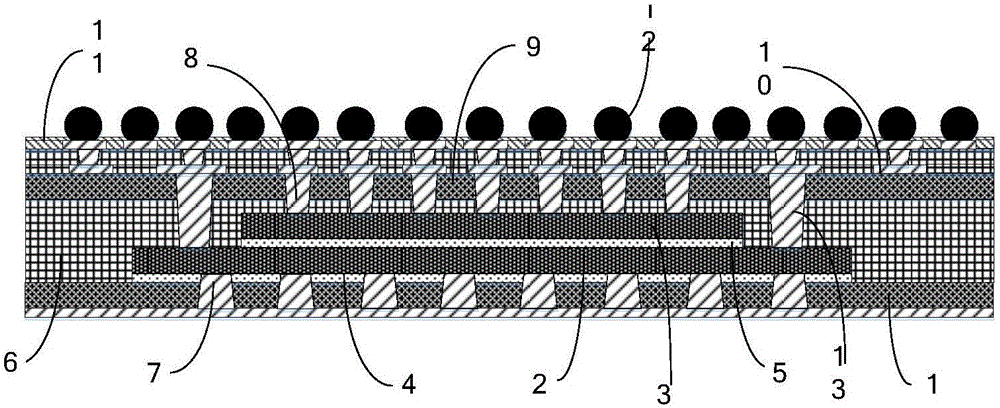
[0037] Such as figure 1 with Figure 8 As shown: in order to achieve a high degree of packaging integration, reduce packaging costs, and be suitable for large-scale mass production requirements, the present invention includes a lower organic core board 1, and multiple layers are laminated on the lower organic core board 1 through a dielectric layer 6 Chip, the multi-layer chip is supported in the lower organic chip 1 and is located in the dielectric layer 6; solder balls 12 for electrical connection with the multi-layer chip are arranged above the dielectric layer 6; heat dissipation columns are arranged in the lower organic core board 1 7. The heat dissipation column 7 penetrates the lower organic core board 1 and contacts the chips adjacent to the lower organic core board 1 .

[0038] Specifically, the heat dissipation column 7 may be a copper column, and t...


PUM


Abstract

The invention relates to a fan-out type packaging structure and a packaging method, in particular to a fan-out type packaging structure based on multiple layers of chips of an organic substrate and a packaging method, and belongs to the technical field of microelectronic packaging. According to the technical scheme, the fan-out type packaging structure based on the multiple layers of chips of the organic substrate comprises a lower organic core board. The chips are laminated on the lower organic core board through dielectric layers, supported in the lower organic core board and located in the dielectric layers. Welding balls electrically connected with the chips are arranged above the dielectric layers. A heat-dissipating column is arranged in the lower organic core board, penetrates through the lower organic core board, and makes contact with the chips adjacent to the lower organic core board. The packaging structure is compact, high in packaging integration degree, suitable for large-scale mass production, safe and reliable, and reduces the packaging cost, and the process is convenient to operate.

Description

technical field [0001] The invention relates to a fan-out packaging structure and a packaging method, in particular to a fan-out packaging structure and a packaging method of a multilayer chip based on an organic substrate, and belongs to the technical field of microelectronic packaging. Background technique [0002] The current fan-out packaging technology is mainly based on the plastic packaging and wafer technology of packaging factories. There are relatively few technologies based on organic substrates. The fan-out packaging based on plastic packaging and wafer technology mainly has low processing costs and wide application range. Small and other shortcomings, it is difficult to apply to large-scale mass production requirements. Contents of the invention [0003] The purpose of the present invention is to overcome the deficiencies in the prior art, and provide a fan-out packaging structure and packaging method for multilayer chips based on an organic substrate, which h...

Claims


Application Information

Patent Timeline
IPC IPC(8): H01L25/18H01L51/10H01L51/40H01L51/44H01L51/48H01L51/52H01L51/56
CPCH01L2224/73267H01L2224/92144H01L2224/92244H01L2924/3025Y02E10/549H01L2224/04105H01L2224/12105H01L2224/2518H01L2224/32145H01L2224/32225H01L2224/73217Y02P70/50H01L2924/3511
Inventor 郭学平刘丰满
Owner NAT CENT FOR ADVANCED PACKAGING
Learn More