Method for adding redundancy patterns to photoetching map

A technology of redundant graphics and layout, applied in special data processing applications, instruments, electrical digital data processing, etc., can solve problems such as graphics depression, reduce defects, avoid copper wire damage, and improve product qualification rates.

Inactive Publication Date: 2015-03-25
SHANGHAI HUALI MICROELECTRONICS CORP
View PDF7 Cites 8 Cited by
  • Summary
  • Abstract
  • Description
  • Claims
  • Application Information

AI Technical Summary

Problems solved by technology

[0008] This patent mainly solves the problem of flatness of metal tungsten in the CMP process, but does not involve how to solve the problem of pattern depression caused by CMP when the pattern area on the surface of the wafer is uneven

Method used


Image

  • Method for adding redundancy patterns to photoetching map
  • Method for adding redundancy patterns to photoetching map
  • Method for adding redundancy patterns to photoetching map

Examples


Embodiment Construction

[0031] The invention provides a method for designing a lithographic layout, which can be applied to processes with technology nodes of 90nm, 65 / 55nm, 45 / 40nm, 32 / 28nm, greater than or equal to 130nm, and less than or equal to 22nm; it can be applied to the following technical platforms : Logic, Memory, RF, HV, Analog / Power, MEMS, CIS, Flash and eFlash.
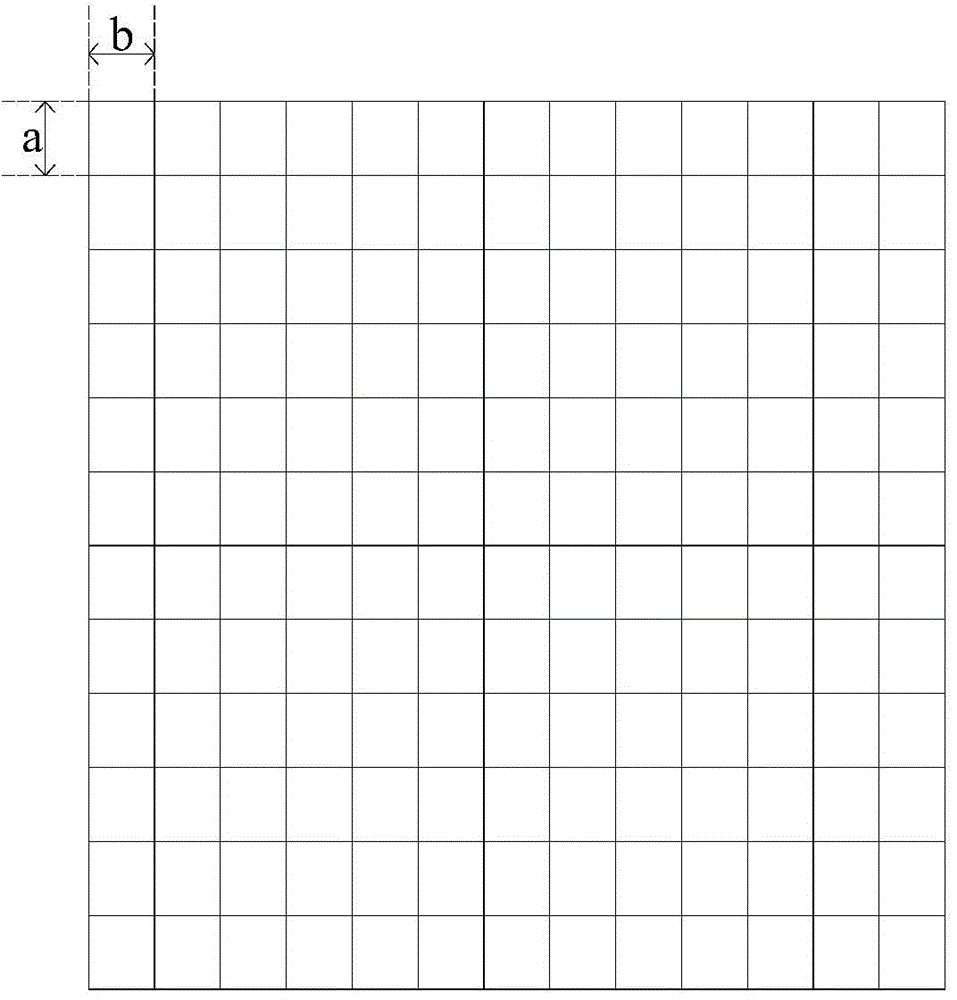
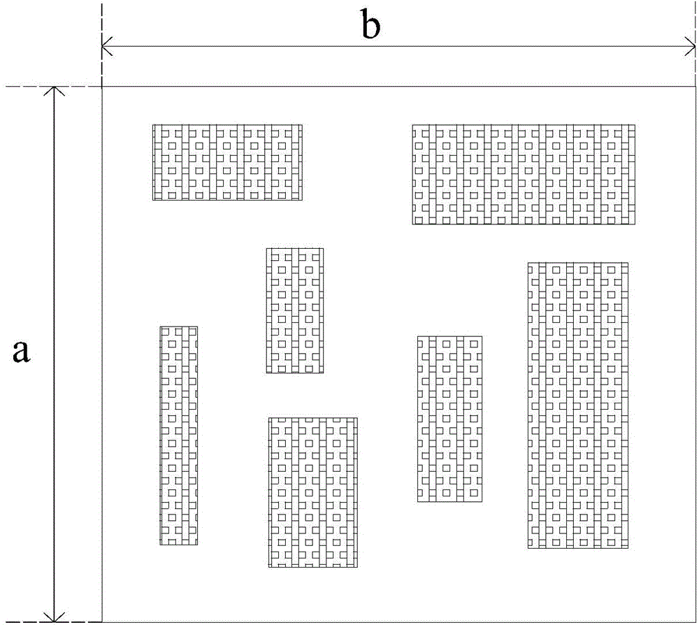
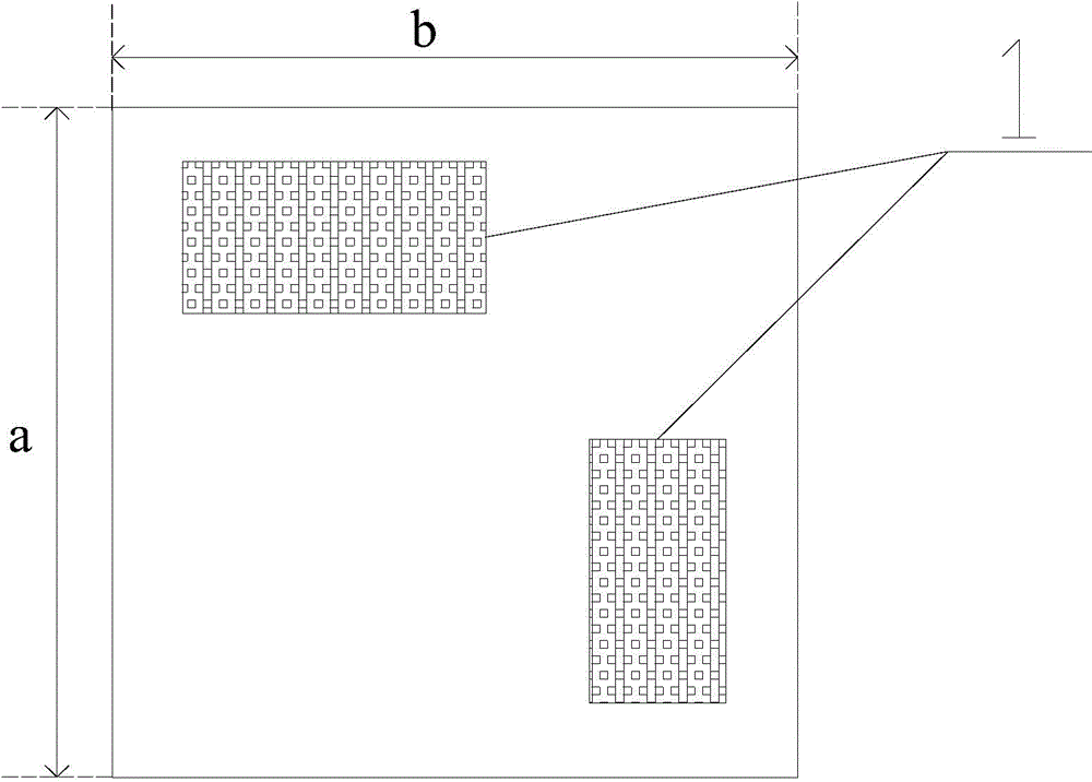
[0032] The core idea of ​​the present invention is by dividing the layout of the completed device design into several areas, and obtaining the ratio of the area occupied by all design graphics on each area to the total perimeter of all design graphics, and then respectively passing The above data of each area judge whether to add redundant graphics to each area separately, and finally make the area density and number density distribution of the graphics on the entire wafer uniform, so that when the wafer is undergoing the CMP process, the grinding The speed is consistent, avoiding the problems of erosion and dishing on the waf...


PUM


Abstract

The invention provides a method for adding redundancy patterns to a photoetching map. The method comprises the steps that S1 the photoetching map containing multiple design patterns is provided, and the photoetching map is divided into at least two areas; S2 the total area, the total perimeter and the region area of the design pattern in each area are obtained; S3 the ratio of the total area and the region area of the design pattern in each area is obtained through calculation; S4 all areas with the correlative value within(A,1)are not filled with the redundancy patterns, all areas with the correlative value smaller than A are filled according to the principle that the smaller the total perimeter is, the larger the filled redundancy pattern is, and the ratio of the total area of the design pattern and the corresponding redundancy pattern in any area and the region area of the area is within(A,1), and the value range of A is within (0,1). The method enables the surface density distribution of a wafer to be more even, and a chemical mechanical grinding effect is improved.

Description

technical field [0001] The invention relates to the field of wafer manufacturing, in particular to a method for adding redundant graphics in a photolithography layout. Background technique [0002] In the 1970s, multi-layer metallization technology was introduced into the integrated circuit manufacturing process. This technology enables the effective use of the vertical space of the chip and improves the integration of the device. However, this technology aggravates the unevenness of the surface of the silicon wafer, and a series of problems caused by it (such as causing uneven thickness of the photoresist and resulting in limitation of lithography) have seriously affected the development of large-scale integrated circuits (LSI). In response to this problem, the industry has successively developed a variety of planarization technologies, mainly including back-etching, glass reflow, spin-coating, etc., but the effect is not ideal. In the late 1980s, IBM Corporation developed...

Claims


Application Information

Patent Timeline
Patent Type & Authority Applications(China)
IPC IPC(8): H01L27/02G06F17/50
Inventor 倪晟于世瑞毛智彪张瑜
Owner SHANGHAI HUALI MICROELECTRONICS CORP
Why Eureka
Try Eureka