Three-group nitride micro-nano light-emitting device with embedded active layer and manufacturing method

A technology of light-emitting devices and nitrides, applied in semiconductor devices, electrical components, circuits, etc., can solve the problems of random distribution of positions, low quantum efficiency, poor size uniformity of quantum dots, etc., and achieve controllable position and size, high quantum efficiency. Effect

Active Publication Date: 2015-03-25
SUN YAT SEN UNIV
View PDF5 Cites 10 Cited by
  • Summary
  • Abstract
  • Description
  • Claims
  • Application Information

AI Technical Summary

Problems solved by technology

[0005] In order to solve the problem of low quantum efficiency caused by dislocations in the Group-III nitride-based optoelectronic materials of light-emitting devices in the prior art, the present invention first proposes a Group-III nitride micro-nano light-emitting device with an embedded active layer. layer grown on a dislocation-free region III-nitride substrate material with extremely high quantum efficiency
[0006] Another object of the present invention is to propose a preparation method of a group-III nitride micro-nano light-emitting device with an embedded active layer, which solves the problem of low quantum efficiency caused by dislocations and InGaN quantum During the dot growth process, problems such as random distribution of positions and poor size uniformity of quantum dots are faced. By controlling the preparation process, the position and size of the active layer can be controlled, and an electroluminescent InGaN quantum dot light source can be realized.

Method used


Image

  • Three-group nitride micro-nano light-emitting device with embedded active layer and manufacturing method
  • Three-group nitride micro-nano light-emitting device with embedded active layer and manufacturing method
  • Three-group nitride micro-nano light-emitting device with embedded active layer and manufacturing method

Examples


Embodiment 1

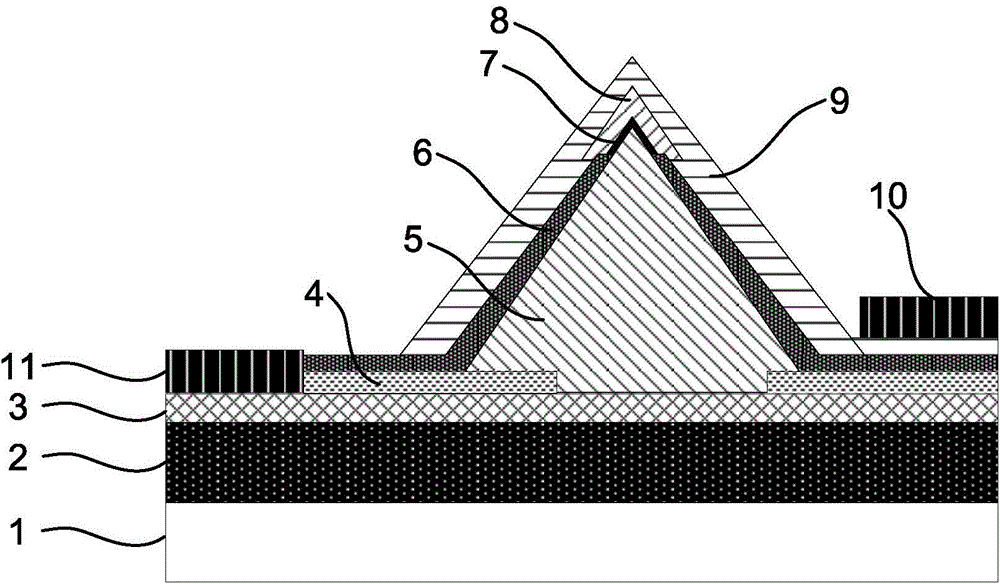
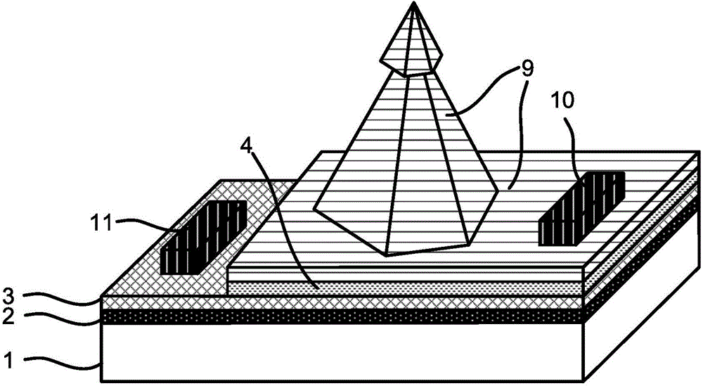
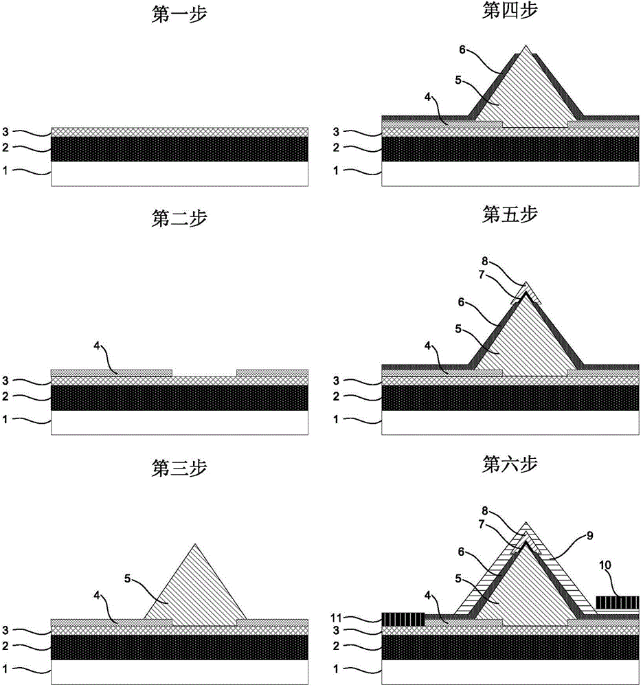
[0055] As shown in Figure 1, a Group III nitride light-emitting device with an embedded active layer, including an initial light-emitting device, a transparent conductive layer 9, a p-type electrode 10 and an n-type electrode 11;

[0056] Among them, the initial light-emitting device has a substrate 1, a nucleation layer and a buffer layer 2 of the III-nitride compound, an n-type III-nitride compound layer 3, a patterned masking film 4, and an n-type III-nitride compound for selective epitaxial growth from bottom to top. The nitride structure 5, the masking film 6 exposing the top of the selectively epitaxially grown n-type III-nitride structure, the III-group nitride active layer 7 and the p-type III-group nitride capping layer 8; wherein the III-group nitride active layer Layer 7 is arranged between the selectively epitaxially grown n-type III-group nitride structure 5 not covered by the masking film (6) and the p-type III-group nitride covering layer 8; wherein the selective...

Embodiment 2

[0068] This embodiment adopts the same device structure and preparation process as in Embodiment 1, wherein the nucleation AlN layer and buffer AlGaN layer in Embodiment 1, and the n-type GaN layer are replaced by the n-type AlGaN conductive nucleation in Embodiment 2 Layer 201. In addition, the front n-type electrode in Example 1 is replaced by the back n-type electrode at the bottom of the Si substrate in Example 2, thus successfully preparing a vertical conductor in which current is injected from the p-type electrode and flows out from the back n-type electrode. A single independent III-nitride micro-nano light-emitting device embedded with an InGaN active layer driven by electricity.

Embodiment 3

[0070] This embodiment adopts the epitaxial structure, device structure, and manufacturing process that are basically the same as those in Embodiment 2, wherein the pattern of the patterned masking film 4 in Embodiment 2 is changed to a periodic pattern with a period of 60 μm, a width of 5 μm, and a length of 500 μm. strip structure, while replacing the n-type GaN-based hexagonal pyramid structure in the epitaxial structure with the n-type GaN-based strip structure (trapezoid in cross section) in Embodiment 3. Similarly, the InGaN active layer 7 and the p-type GaN-based striped cladding layer (triangular in cross section) are epitaxially grown in sequence at the apex of the n-type GaN-based strip structure (trapezoidal in cross section) not covered by the masking film. ). This embodiment is a single independent Group III nitride micro-nano light-emitting device embedded with an InGaN active layer driven by vertical conduction of current injected from the p-type electrode and f...


PUM

PropertyMeasurementUnit
thicknessaaaaaaaaaa
thicknessaaaaaaaaaa

Abstract

The invention discloses a three-group nitride micro-nano light-emitting device with an embedded active layer and a manufacturing method. The light-emitting device comprises an initial light-emitting device, a transparent conducting layer, a p-type electrode and an n-type electrode; the initial light-emitting device is sequentially provided with a substrate, a three-group nitride nucleating layer, a buffering layer, an n-type three-group nitride layer, imaging 5 masking film, a selective epitaxial growth n-type three-group nitride structure, selective epitaxial growth exposed masking film at the top of the n-type three-group nitride structure, the three-group nitride active layer and a p-type three-group nitride coverage layer from bottom to top. The three-group nitride active layer is arranged between a part, which is not masked and covered, between the selective epitaxial growth n-type three-group nitride structure and the p-type three-group nitride coverage layer; the transparent conducting layer is deposited to the front face of the initial light-emitting device, the p-type electrode is arranged on the transparent conducting layer, and the n-type electrode is arranged on the n-type three-group nitride layer or the bottom of the substrate. The light-emitting device (10) has the advantages of being controllable in position and size, stable in performance and ultra high in quantum efficiency.

Description

technical field [0001] The invention relates to the field of semiconductor light-emitting devices, in particular to a Group III nitride micro-nano light-emitting device with an embedded active layer and a preparation method. Background technique [0002] Group-III nitrides (III-N) have become a hotspot in the research of semiconductor technology due to their characteristics of wide band gap, high thermal conductivity, high electron saturation drift velocity and large critical breakdown voltage. Group III nitrides GaN, AlN (bandgap 6.2eV), InN (bandgap 0.7eV) and their alloys cover the energy range from infrared to visible light and ultraviolet light, so they have a wide range of applications in the field of optoelectronics. Applications, such as high-power white LEDs, lasers, solar-blind detectors in the ultraviolet band, etc. At present, III-N-based LEDs, LDs and electronic devices have achieved commercial production, and are widely used in display backlight, lighting, inf...

Claims


Application Information

Patent Timeline
Patent Type & Authority Applications(China)
IPC IPC(8): H01L33/30H01L33/32H01L33/12
CPCH01L33/0075H01L33/12H01L33/30H01L33/32H01L2933/0008
Inventor 张佰君陈伟杰林佳利胡国亨
Owner SUN YAT SEN UNIV
Why Eureka
Try Eureka