Device for converting rectangular waveguide into substrate integrated waveguide at Ka wave band

A substrate-integrated waveguide, rectangular waveguide technology, applied in the direction of connection devices, waveguide devices, electrical components, etc., can solve the problems of difficult processing, large circuit size, large insertion loss, etc., and achieve convenient processing and reduced circuit size Effect

Inactive Publication Date: 2015-03-25
UNIV OF ELECTRONICS SCI & TECH OF CHINA
View PDF2 Cites 7 Cited by
  • Summary
  • Abstract
  • Description
  • Claims
  • Application Information

AI Technical Summary

Problems solved by technology

For example, in the literature Zhong C L, Xu J and Zhi Z Y 2009 Electron.Lett.45205 and Li J, Wen G and Xiao F 2010 Electron.Lett.46 223, the antipolar fin line is used to realize the transition, as shown in Figure (1). But the length of the tapered fin line makes the circuit size larger
However, the transition structure based on the ridge-shaped stepped waveguide proposed in the literature Li T, Meng H F and Dou W B 2014 IEICE Electron.Express 11 1, although the circuit size is small, the insertion loss is slightly larger, and it is not easy to process

Method used


Image

  • Device for converting rectangular waveguide into substrate integrated waveguide at Ka wave band
  • Device for converting rectangular waveguide into substrate integrated waveguide at Ka wave band
  • Device for converting rectangular waveguide into substrate integrated waveguide at Ka wave band

Examples


Embodiment Construction

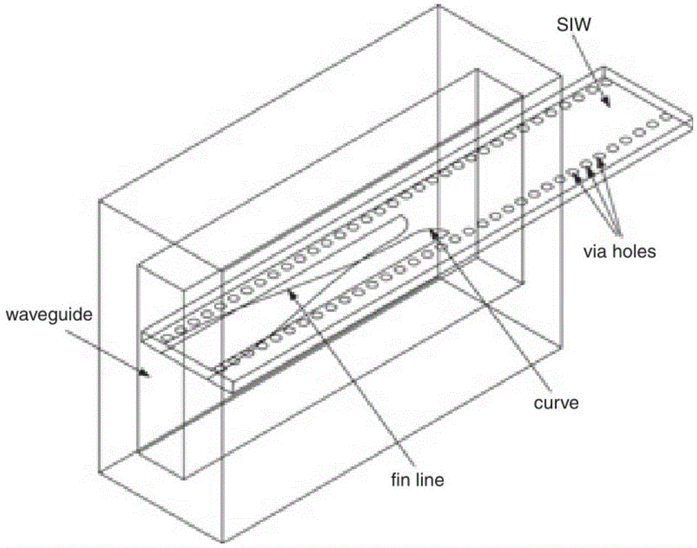
[0013] This patent is further described in conjunction with the accompanying drawings.

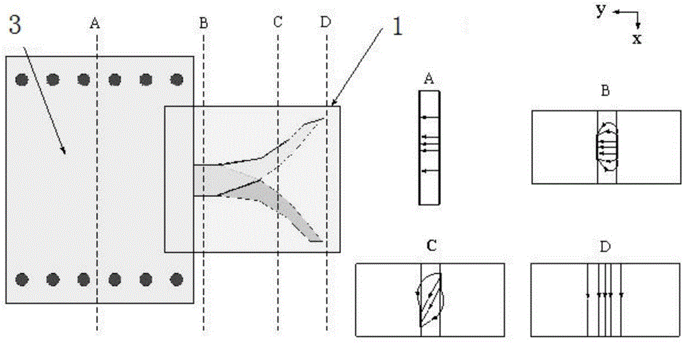
[0014] At first this design needs modeling and optimization in special-purpose electromagnetic simulation software, the present invention adopts the high-frequency structural simulation software (HFSS) of Ansoft Company to carry out modeling simulation, by image 3 The tuning and simulation optimization of each parameter in , to obtain the optimal solution, the finally determined parameter size is r=0.2mm, d=0.78mm, W siw =4.85mm, W 0 = 0.72mm, W 1 =0.51mm, W 2 =0.3mm, W=1.12mm, L=3.12mm, the length of the entire transition structure is only 3.6mm. After the design is completed, it is processed and finally tested.

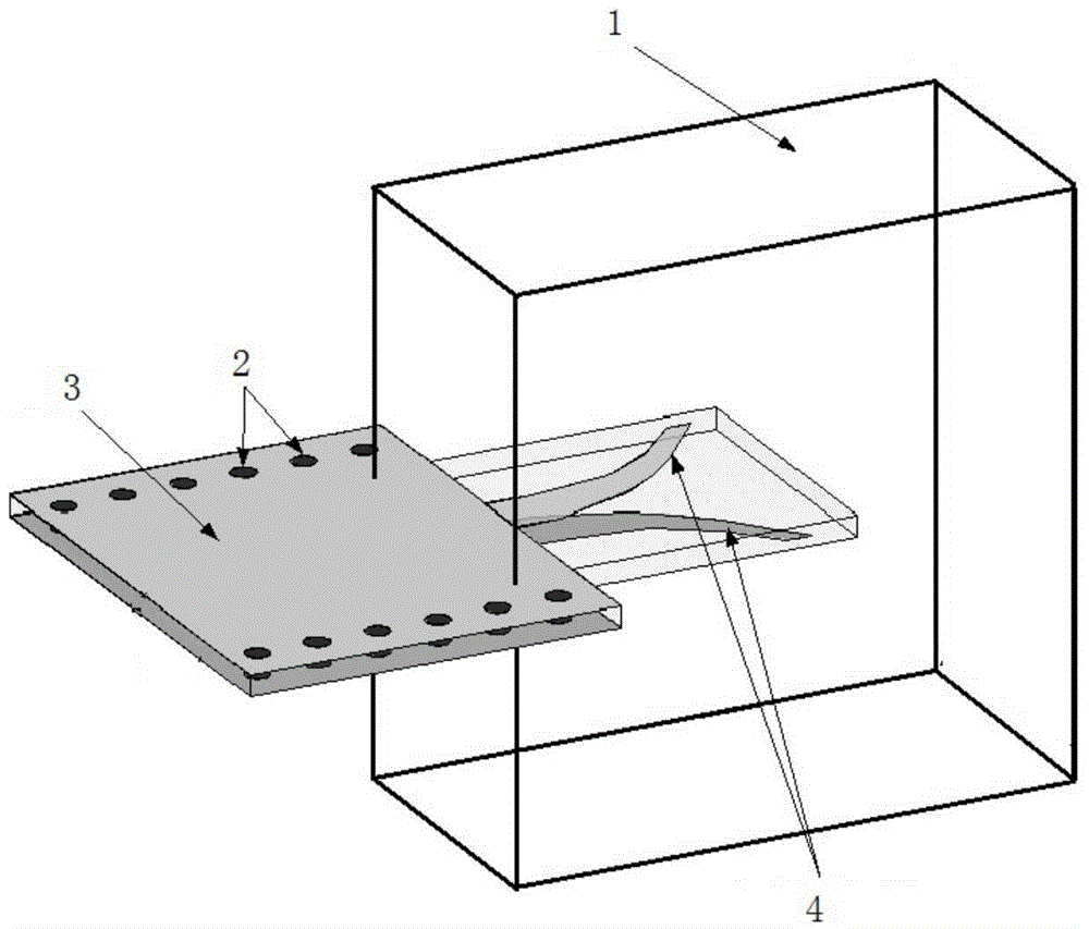
[0015] The working principle of the present invention: the transition structure is based on the E-plane probe coupling, and the antisymmetric tapered probe is used to realize the TE of the main mode of the rectangular waveguide 10 Die-to-substrate integrated waveguide (SIW...


PUM


Abstract

The invention discloses a device for converting a rectangular waveguide into a substrate integrated waveguide at the Ka wave band, belongs to the technical field of microwave millimeter wave integration, and particularly relates to a novel small transition structure for converting the rectangular waveguide into the substrate integrated waveguide at the Ka wave band. The device comprises the WR-28 rectangular waveguide, a transition structure and the substrate integrated waveguide (SIW). The transition structure comprises a dielectric substrate and flaky probes located on the upper layer and the lower layer of the dielectric substrate respectively, and the probes on the upper layer and the lower layer are bent conical flaky probes bent towards two sides. Thus, the device for converting the rectangular waveguide into the substrate integrated waveguide at the Ka wave band has the advantages that the return loss is better than 15 dB, the insertion loss is smaller than 1.4 dB, the work bandwidth is 24-40 GHz, the test result is similar to a simulation result, the circuit size is largely reduced and is only 3.6 mm long, and machining is quite convenient.

Description

technical field [0001] The invention belongs to the technical field of microwave and millimeter wave integration, in particular to a novel miniaturized rectangular waveguide-to-substrate integrated waveguide transition structure applied to the Ka wave band. Background technique [0002] Substrate integrated waveguide is a high-performance, low-loss miniaturized transmission line proposed in recent years, and it is easy to integrate with planar circuits. Many advantages make substrate integrated waveguides become future circuits in the field of microwave and millimeter wave circuits. development trend. This printed planar technology has been widely used in microwave and millimeter wave components and subsystems, such as filters, antennas, transition structures, couplers, power splitters, polarization rotators, and oscillators. In addition, the air-filled rectangular waveguide has the advantages of high Q value and large power capacity, making it an important transmission lin...

Claims


Application Information

Patent Timeline
Patent Type & Authority Applications(China)
IPC IPC(8): H01P5/08
Inventor 董俊刘宇杨涛杨自强汪子成
Owner UNIV OF ELECTRONICS SCI & TECH OF CHINA
Why Eureka
Try Eureka