A laser etching method for transparent conductive film

A technology of transparent conductive film and laser etching method, applied in laser welding equipment, welding equipment, metal processing equipment, etc., can solve the problems of complex realization and high requirements for laser focusing accuracy, and achieve the requirements of reducing laser focusing accuracy and reliability. Good, easy-to-use effects

Active Publication Date: 2016-08-24
杭州银湖激光科技有限公司
View PDF9 Cites 0 Cited by
  • Summary
  • Abstract
  • Description
  • Claims
  • Application Information

AI Technical Summary

Problems solved by technology

[0010] The purpose of the present invention is to provide a laser etching method for transparent conductive films, which overcomes the problems of high laser focus accuracy and complex implementation in the prior art

Method used


Image

  • A laser etching method for transparent conductive film
  • A laser etching method for transparent conductive film
  • A laser etching method for transparent conductive film

Examples


Embodiment 1

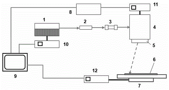
[0029] Example 1: see figure 1 As shown, a laser etching method for a transparent conductive film includes the following steps:

[0030] (1) A short-wavelength infrared pulse laser is used to output pulsed lasers with a wavelength between 1.4 μm and 3.0 μm, with a pulse width of 0.1 ns to 800 ns, and collimation processing is performed. The short-wavelength infrared pulse laser is a fiber laser, single pulse The laser energy is 1 to 2000 microjoules, and the pulse frequency is 1 kilohertz to 1 megahertz;

[0031] (2) The pulsed laser beam is irradiated on the transparent conductive film placed on the two-dimensional translation stage, and the relative movement of the laser beam and the two-dimensional translation stage is controlled to make the laser beam focus on the transparent conductive film and move according to the set path. For etching, control the relative movement speed of the laser and the transparent conductive film to 50mm / s~9000mm / s, and the overlap degree of the light...

Embodiment 2

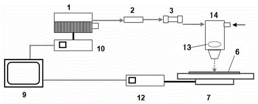
[0033] Example 2: see figure 2 As shown, a laser etching method for a transparent conductive film includes the following steps:

[0034] (1) A short-wavelength infrared pulse laser is used to output pulsed lasers with a wavelength between 1.4 μm and 3.0 μm, with a pulse width of 0.1 ns to 800 ns, and collimation processing is performed. The short-wavelength infrared pulse laser is a fiber laser, single pulse The laser energy is 1 to 2000 microjoules, and the pulse frequency is 1 kilohertz to 1 megahertz;

[0035] (2) The pulsed laser beam is irradiated on the transparent conductive film placed on the two-dimensional translation stage, and the relative movement of the laser beam and the two-dimensional translation stage is controlled to make the laser beam focus on the transparent conductive film and move according to the set path. For etching, control the relative movement speed of the laser and the transparent conductive film to 50mm / s~9000mm / s, and the overlap degree of the ligh...


PUM

PropertyMeasurementUnit
wavelengthaaaaaaaaaa

Abstract

The invention discloses a laser etching method of a transparent conductive thin film. The method comprises the following steps of (1) outputting pulse laser beams with an output wavelength of 1.4-3.0 mu m through a short-wave long-infrared pulse laser device at a pulse width of 0.1-800 ns, and performing collimation treatment, wherein the short-wave long-infrared pulse laser device is an optical fiber laser device and has a single-pulse laser power capacity of 1-2000 microjoules and a pulse frequency of 1 KHz-1 MHz; (2) enabling the laser beams to illuminate a film substrate on a two-dimensional moving table, controlling the relative movement of the laser beams and the two-dimensional moving table to enable the focus point of the laser beams to move on the transparent conductive thin film according to a set path to perform etching, and controlling the laser beams and the transparent conductive thin film to move relatively as a speed of 50-9000 mm / s and to have a spot overlapping degree of 10-90%. The laser etching method of the transparent conductive thin film can overcome the problems of high laser focusing precision requirements and implementing complexity in the prior art.

Description

Technical field [0001] The invention relates to a laser processing and preparation method of a transparent conductive film, in particular to a method for laser etching the film layer of the transparent conductive film. Background technique [0002] Transparent conductive film is a kind of film that can conduct electricity and has high transparency in the visible light range. It mainly includes metal film system, oxide film system, other compound film system, polymer film system, and composite film system. The metal film has good electrical conductivity but poor transparency. The semiconductor film series are just the opposite, with poor conductivity and high transparency. At present, the most widely studied and applied are metal film systems and oxide film systems. Common transparent conductive films are ITO (tin doped indium trioxide), AZO (aluminum doped zinc oxide), etc. They have a large band gap and do not absorb visible light, so they are called "transparent". [0003] ITO...

Claims


Application Information

Patent Timeline
Patent Type & Authority Patents(China)
IPC IPC(8): B23K26/362
Inventor 蒋仕彬
Owner 杭州银湖激光科技有限公司
Why Eureka
Try Eureka