Supercharge Your Innovation With Domain-Expert AI Agents!

Three-dimensional on-chip optical network topology and routing path calculation method

A technology of network topology and path calculation, applied in the field of communication, can solve the problems of waste of chip resources, redundant deployment of optical router components, large transmission delay at zero load, etc., and achieve the effect of reducing chip area and reducing chip resource consumption.

Active Publication Date: 2017-07-25
NORTHEASTERN UNIV LIAONING
View PDF4 Cites 0 Cited by
  • Summary
  • Abstract
  • Description
  • Claims
  • Application Information

AI Technical Summary

Problems solved by technology

[0006] The existing three-dimensional on-chip optical network uses a network topology structure, which has the problem of large zero-load transmission delay. In addition, the current three-dimensional on-chip network mostly uses homogeneous optical routers, and the deployment of components inside each optical router is relatively redundant. As a result, chip resources such as optical crossbar switches are seriously wasted
[0007] For the routing algorithm of 3D on-chip network, dimension order routing is widely used. However, this routing algorithm can only calculate a macroscopic optical path for each packet message, and the microscopic packet message forwarding path inside each node through which the optical path passes cannot be determined. computational

Method used


Image

  • Three-dimensional on-chip optical network topology and routing path calculation method
  • Three-dimensional on-chip optical network topology and routing path calculation method
  • Three-dimensional on-chip optical network topology and routing path calculation method

Examples


Embodiment Construction

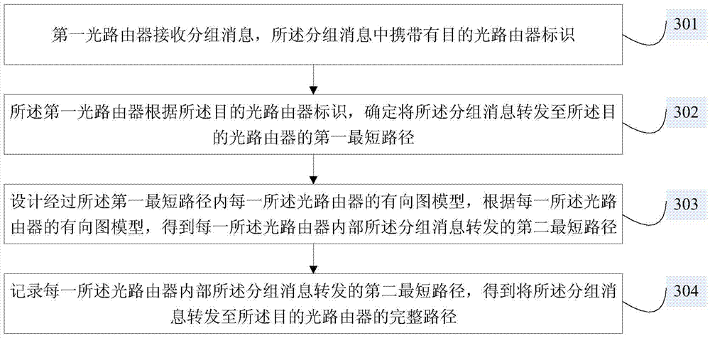
[0044] The specific implementation manners of the present invention will be further described below in conjunction with the drawings and examples. The following examples are used to illustrate the present invention, but are not intended to limit the scope of the present invention.

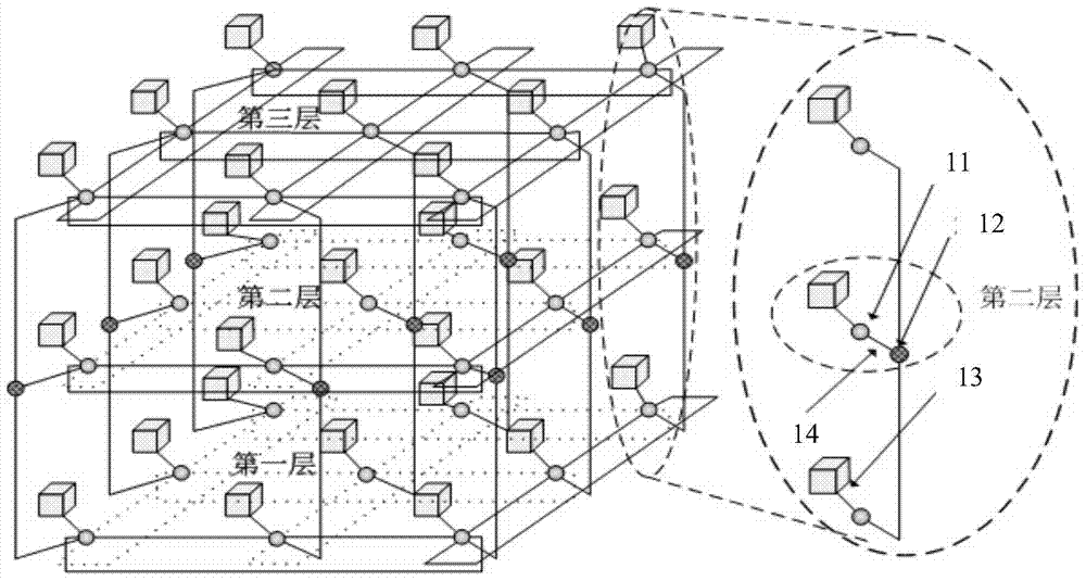
[0045] The three-dimensional on-chip optical network topology of this embodiment may include: N optical routing layers, each of which includes N rows×N columns of optical routers, each of which is connected to an IP core, at least one Each of the optical routers in the optical routing layer is also connected to a vertical optical router;

[0046] Wherein, the N is a natural number greater than or equal to 3.

[0047] Further, each of the optical routing layers is a loop topology, and the connection of the optical routers in each of the optical routing layers is:

[0048] Each of the optical routers is connected to adjacent optical routers, and the first optical router in each row or column is als...


PUM


Abstract

The present invention provides a three-dimensional on-chip optical network topology and a routing path calculation method. The three-dimensional on-chip optical network topology includes: N optical routing layers, each of which includes N rows×N columns of optical routers, each The optical router is connected to an IP core, and each optical router of at least one optical routing layer is connected to a vertical optical router, wherein, the N is a natural number greater than or equal to 3. Each of the optical routers is connected to adjacent optical routers, and the first optical router in each row or column is also connected to the last optical router in the row or column, and each of the vertical optical routers is connected to another optical router. The optical routers at corresponding positions in the two optical routing layers are connected, thereby reducing chip resource consumption and reducing the maximum chip area.

Description

[0001] Technical field: [0002] The invention relates to communication technology, in particular to a three-dimensional on-chip optical network topology and a routing path calculation method. [0003] Background technique: [0004] In the mid-1990s, integrated circuits began to transform into integrated systems, and SoCs came into being. System-on-chip integrates various types of integrated circuits into a single chip, making system-level products portable. However, with the rapid development of CMOS technology, it is urgent to design a new architecture to relieve the communication pressure of the system on chip by decoupling various types of integrated circuits from the shared bus channel. The network on chip is to implant computer network technology into the chip design, which fundamentally solves the above-mentioned communication problem of the system on chip based on the shared bus. However, as the number of IP cores in a single chip continues to increase, the high energ...

Claims


Application Information

Patent Timeline
Patent Type & Authority Patents(China)
IPC IPC(8): H04L12/701
Inventor 侯维刚郭磊宋清洋于尧刘业君吴菁晶彭玉怀巩小雪
Owner NORTHEASTERN UNIV LIAONING
Features
  • R&D
  • Intellectual Property
  • Life Sciences
  • Materials
  • Tech Scout
  • Unparalleled Data Quality
  • Higher Quality Content
  • 60% Fewer Hallucinations
Learn More