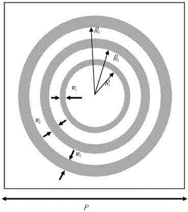
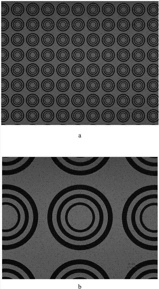
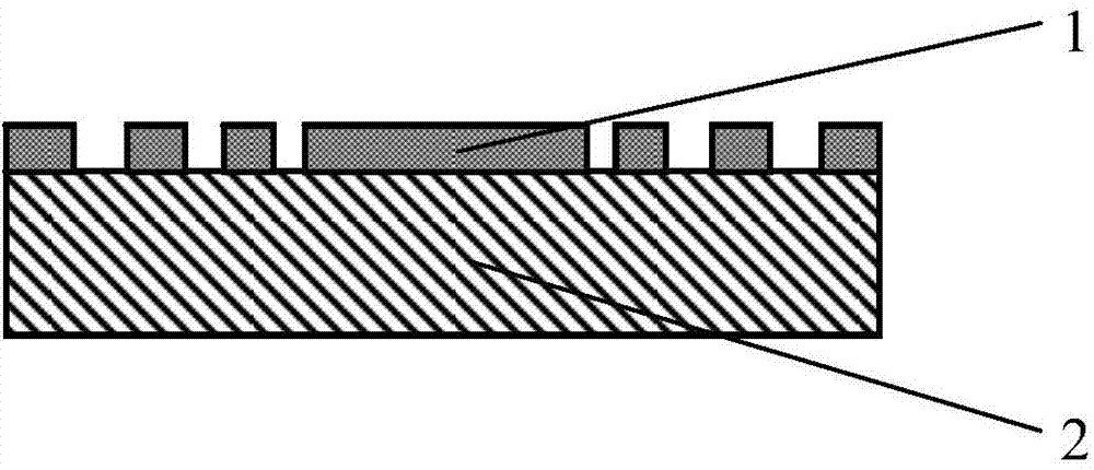
Multiband terahertz filter and manufacture method of multiband terahertz filter
A manufacturing method and terahertz technology, which are applied in the terahertz field to achieve the effects of large polarization insensitivity, good out-of-band suppression performance, and ingenious design ideas.
- Summary
- Abstract
- Description
- Claims
- Application Information
AI Technical Summary
Problems solved by technology
Method used
Image
Examples
Embodiment 1
[0067] A 3-band terahertz filter made by the following method:
[0068] Step 1: cleaning the single crystal Z-cut quartz substrate;
[0069] In this step, the cleaning process is as follows:
[0070] (1) Put the quartz substrate into the acetone solution, and ultrasonically clean it for 5-10 minutes;
[0071] (2) Take out the substrate and put it into isopropanol (IPA) for ultrasonic cleaning for 5-10 minutes;
[0072] (3) Take out the substrate and clean it with deionized water, and dry the substrate with a nitrogen gun;
[0073] Step 2: depositing a metal aluminum (Al) film layer on the cleaned quartz substrate;
[0074] In this step, magnetron sputtering technology is used to deposit a 200nm thick metal aluminum film layer on the cleaned quartz substrate at room temperature; a metal film with a thickness of more than 200nm can ensure that it does not pass through electromagnetic waves; magnetron sputtering is a new technology in the field Routine operation, no more deta...
Embodiment 2
[0091] A 3-band terahertz filter made by the following method:
[0092] Step 1: cleaning the quartz substrate;
[0093] In this step, the cleaning process is as follows:
[0094] (1) Put the quartz substrate into the acetone solution, and ultrasonically clean it for 5-10 minutes;
[0095] (2) Take out the substrate and put it into isopropanol (IPA) for ultrasonic cleaning for 5-10 minutes;
[0096] (3) Take out the substrate and clean it with deionized water, and dry the substrate with a nitrogen gun;
[0097] Step 2: Spin-coat optical photoresist on the quartz substrate and bake;
[0098] In this step, first place the sample on a hot plate and bake at 120°C for 10 minutes to remove the moisture on the surface, then spin-coat S1813 photoresist with a thickness of about 1 μm, and place it in an oven for 40 minutes at 110°C;
[0099] Step 3: Exposure and development to obtain a periodic 3-ring structure pattern of the photoresist;
[0100] In this step, the S1813 photoresis...
PUM
 Abstract
Description
Claims
Application Information


