A method of manufacturing a semiconductor device

A technology for semiconductors and devices, applied in the field of manufacturing semiconductor devices, can solve problems such as the inability to meet technical requirements, and achieve the effects of improving the double peak effect, reducing the size in the width direction, and improving performance

Active Publication Date: 2018-07-20
SEMICON MFG INT (SHANGHAI) CORP
View PDF6 Cites 0 Cited by
  • Summary
  • Abstract
  • Description
  • Claims
  • Application Information

AI Technical Summary

Problems solved by technology

According to the existing technology, the rounding process of the corners of the shallow trench isolation structure has limitations, and at the same time, it can no longer meet the growing technical requirements

Method used


Image

  • A method of manufacturing a semiconductor device
  • A method of manufacturing a semiconductor device
  • A method of manufacturing a semiconductor device

Examples


Embodiment Construction

[0025] In the following description, numerous specific details are given in order to provide a more thorough understanding of the present invention. It will be apparent, however, to one skilled in the art that the present invention may be practiced without one or more of these details. In other examples, some technical features known in the art are not described in order to avoid confusion with the present invention.

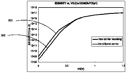
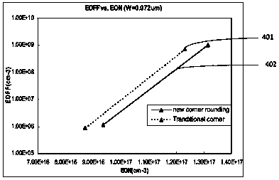
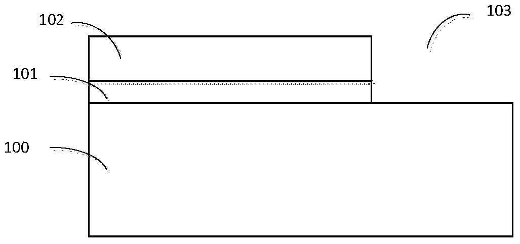
[0026] In order to thoroughly understand the present invention, detailed steps will be proposed in the following description, so as to illustrate how the present invention improves the roundness of the top corner of the shallow trench isolation structure, so as to avoid the generation of leakage current and reduce the impact of the transistor on the shallow trench. The sensitivity of the isolation shape. Apparently, the preferred embodiments of the present invention are described in detail as follows, however, the present invention may also have other implement...


PUM

PropertyMeasurementUnit
thicknessaaaaaaaaaa
thicknessaaaaaaaaaa

Abstract

The invention discloses a semiconductor device production method. The method includes: providing a semiconductor substrate; forming an oxide underlayer and a nitride layer on the semiconductor substrate in sequence; patterning the oxide underlayer and the nitride layer so as to form an opening exposing the semiconductor substrate; etching the semiconductor substrate according to the opening so as to form a shallow trench; forming a liner layer on the bottom and the side wall of the shallow trench; adopting a pull-back process to treat the nitride layer so as to expose part of the oxide underlayer near the top of the shallow trench; performing oxidation to expose the oxide underlayer. In conclusion, according to the production process, the form of the shallow trench in the semiconductor substrate can be optimized, formed STI (shallow trench isolation) corners are rounder and smoother, double hump caused by the fact that transistors of the STI corner areas are opened earlier is improved, performance of the semiconductor device is improved, the size of the semiconductor device in the width direction is reduced favorably, and the shallow trench is filled subsequently favorably.

Description

technical field [0001] The invention relates to a semiconductor manufacturing process, in particular to a method for manufacturing a semiconductor device. Background technique [0002] As the microelectronics process enters the deep submicron stage, in order to realize high-density, high-performance large-scale integrated circuits, the isolation process between semiconductor devices becomes more and more important. The prior art generally adopts shallow trench isolation technology (STI, Shallow Trench Isolation) to realize the isolation of active devices, such as in complementary metal oxide semiconductor (CMOS) devices, NMOS (N-type metal oxide semiconductor) transistors and PMOS ( The isolation layers between the P-type metal oxide semiconductor) transistors are all formed by shallow trench isolation technology. [0003] Shallow trench isolation technology has gradually replaced other isolation methods used in traditional semiconductor device manufacturing, such as local ...

Claims


Application Information

Patent Timeline
Patent Type & Authority Patents(China)
IPC IPC(8): H01L21/762
Inventor 蒲月皎宋化龙董金珠
Owner SEMICON MFG INT (SHANGHAI) CORP
Why Eureka
Try Eureka