
Semiconductor element, semiconductor device, method for manufacturing semiconductor element, and method for manufacturing semiconductor device

A semiconductor and component technology, applied in the fields of semiconductor/solid-state device manufacturing, semiconductor/solid-state device components, semiconductor devices, etc., can solve the problems of hindering the operation of components, not yet practical, and low resistance, and achieve the effect of improving ESD resistance

Inactive Publication Date: 2015-04-15
KK TOSHIBA
View PDF4 Cites 0 Cited by
  • Summary
  • Abstract
  • Description
  • Claims
  • Application Information

AI Technical Summary

Problems solved by technology

[0004] For example, semiconductor elements such as HEMT (High Electron Mobility Transistor: High Electron Mobility Transistor) are suitable for high-speed operation due to their small gate capacitance, but on the other hand, they have low resistance to ESD (electro-static discharge: electrostatic discharge)
As an ESD countermeasure for devices, it is conceivable to embed protection diodes in the device, but this will increase the device area and hinder the operation of the device, so it has not been put into practical use.

Method used


Image

  • Semiconductor element, semiconductor device, method for manufacturing semiconductor element, and method for manufacturing semiconductor device
  • Semiconductor element, semiconductor device, method for manufacturing semiconductor element, and method for manufacturing semiconductor device
  • Semiconductor element, semiconductor device, method for manufacturing semiconductor element, and method for manufacturing semiconductor device

Examples


no. 1 approach

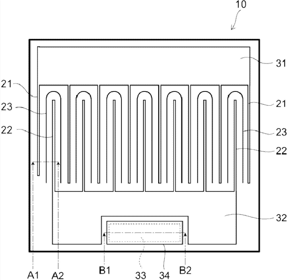
[0029] figure 1 It is a plan view schematically showing the semiconductor element of the first embodiment. In addition, in this plan view, the insulating layer 19 is omitted.

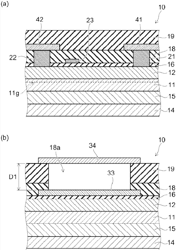
[0030] figure 2 (a) and figure 2 (b) is a partial cross-sectional view schematically showing a part of the semiconductor element of the first embodiment.

[0031] figure 2 (a) Schematic representation figure 1 A1-A2 line section. figure 2 (b) Schematic representation figure 1 B1-B2 line section.

[0032] Such as figure 1 , figure 2 (a) and figure 2 As shown in (b), the semiconductor element 10 has a first semiconductor layer 11, a second semiconductor layer 12, a substrate 14, a base layer 15, a gate insulating film 16, an insulating layer 18 and an insulating layer 19, and a drain electrode 21 (first electrode), source electrode 22 (second electrode), gate electrode 23 (gate electrode), drain junction region 31, source junction region 32, gate junction region 33 (junction region), cond...

no. 2 approach

[0083] Figure 8 (a) and Figure 8 (b) is a schematic diagram showing the semiconductor element of the second embodiment.

[0084] Figure 8 (a) is a partial cross-sectional view schematically showing a part of the semiconductor element 110 .

[0085] Figure 8 (b) is an equivalent circuit diagram schematically showing the semiconductor element 110 .

[0086] Such as Figure 8 As shown in (a), the semiconductor element 110 further includes a resistor 35 . The semiconductor element 110 includes, for example, a plurality of resistors 35 . The resistor 35 is disposed between the gate bonding region 33 and the conductor 34 . The resistor 35 is electrically connected to the gate bonding region 33 and the conductor 34 respectively. Resistor 35 is in contact with gate land 33 and conductor 34 , for example. That is, in the semiconductor element 110 , the conductor 34 is electrically connected to the gate land 33 via the resistor 35 . The resistor 35 is, for example, a metal...

no. 3 approach

[0097] Figure 10 It is a plan view schematically showing the semiconductor element of the third embodiment.

[0098] Figure 11 (a) and Figure 11 (b) is a partial cross-sectional view schematically showing a part of the semiconductor element of the third embodiment.

[0099] Figure 11 (a) Schematic representation Figure 10 The C1-C2 line section.

[0100] Figure 11 (b) Schematic representation Figure 10 D1-D2 line section.

[0101] Such as Figure 10 , Figure 11 (a) and Figure 11 As shown in (b), in the semiconductor element 120 , the opening 18 a and the conductor 34 are provided at positions that do not overlap with the gate bonding region 33 . In the semiconductor element 120 , the opening 18 a and the conductor 34 do not face the gate bonding region 33 .

[0102] In the semiconductor element 120 , the conductor 34 is electrically connected to the gate land 33 via the wiring 36 . In addition, in the semiconductor element 120 , the conductive film 38 is ...


PUM


Abstract

According to one embodiment, a semiconductor element includes a first semiconductor layer, a second semiconductor layer, a first electrode, a second electrode, a control electrode, a pad unit, an insulating layer, and a conductor. The second semiconductor layer is provided on the first semiconductor layer. The first electrode is provided on the second semiconductor layer. The second electrode is provided on the second semiconductor layer. The control electrode is provided on the second semiconductor layer. The pad unit is provided on the second semiconductor layer. The pad unit is electrically connected to the control electrode. The insulating layer is provided on the second semiconductor layer. The insulating layer has an opening. The conductor is provided on the insulating layer. The conductor covers at least a part of the opening.

Description

[0001] Citations from related applications: [0002] This application is based on and claims the priority of the prior Japanese Patent Application No. 2013-207091 filed on October 2, 2013, the entire contents of which are hereby incorporated by reference. technical field [0003] The embodiments described here generally relate to a semiconductor element, a semiconductor device, a method of manufacturing a semiconductor element, and a method of manufacturing a semiconductor device. Background technique [0004] For example, semiconductor elements such as HEMT (High Electron Mobility Transistor: High Electron Mobility Transistor) are suitable for high-speed operation due to their small gate capacitance, but on the other hand, they have low resistance to ESD (electro-static discharge: electrostatic discharge). As an ESD countermeasure for the device, a method of embedding a protection diode in the device can be considered, but this will increase the device area and hinder the o...

Claims


Application Information

Patent Timeline
Patent Type & Authority Applications(China)
IPC IPC(8): H01L29/778H01L21/335H01L29/49
CPCH01L29/66431H01L29/778H01L23/60H01L21/28H01L21/768H01L24/05H01L29/2003H01L29/41758H01L29/42316H01L29/42376H01L29/66462H01L29/7786H01L2224/73265H01L2224/48091H01L2924/12032H01L2924/00014H01L2924/00H01L2924/12042H01L2924/13091H01L2224/92247H01L2224/0603
Inventor 罇贵子
Owner KK TOSHIBA
Learn More