Preparation method of reverse polarity AlGaInP red light LED (Light-Emitting Diode) chip

An LED chip, reverse polarity technology, applied in electrical components, circuits, semiconductor devices, etc., can solve problems such as pollution, and achieve the effect of avoiding pollution, simplifying production processes, and avoiding missing electrodes

Active Publication Date: 2015-04-15
SHANDONG INSPUR HUAGUANG OPTOELECTRONICS
View PDF8 Cites 19 Cited by
  • Summary
  • Abstract
  • Description
  • Claims
  • Application Information

AI Technical Summary

Problems solved by technology

[0006] Aiming at the deficiencies in the existing preparation methods of reverse polarity AlGaInP red LED chips, the present invention proposes a method for preparing chips that can avoid contamination of wafers, reduce missing electrodes, improve production efficiency, and reduce production costs

Method used


Image

  • Preparation method of reverse polarity AlGaInP red light LED (Light-Emitting Diode) chip
  • Preparation method of reverse polarity AlGaInP red light LED (Light-Emitting Diode) chip
  • Preparation method of reverse polarity AlGaInP red light LED (Light-Emitting Diode) chip

Examples


Embodiment Construction

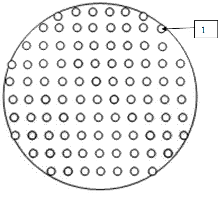
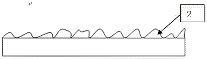
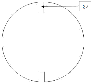
[0023] The preparation method of the GaAs-based light-emitting diode chip of the present invention is to add a step of removing the residual metal film layer on the edge of the wafer after the GaAs substrate is stripped in the existing substrate stripping process, by using tweezers to adjust the position of the wafer, and using a single blade The blade cooperates to remove all the metal film layer remaining on the edge of the wafer. It is ensured that the wafer will not be polluted by metal powder when the N-type electrode is evaporated for the first time, resulting in missing electrodes. When making the registration mark window, the method of sticking high-temperature-resistant tape on the window area is cleverly adopted, and the production of the overlay registration mark window and the evaporation of the N-type electrode are carried out simultaneously, which simplifies the chip production process. The specific process is as follows:

[0024] (1) A layer of TiAu film is eva...


PUM


Abstract

The invention relates to a preparation method of a reverse polarity AlGaInP red light LED (Light-Emitting Diode) chip. The preparation method comprises the following steps: (1) bonding a wafer and a silicon wafer of an GaAs substrate light emitting diode together; (2) corroding an GaAs substrate, rotating the wafer for 180 degrees in the vertical direction and continuously corroding; (3) after the corrosion of the GaAs substrate is completed, scraping a metal film remained on the edge of the wafer; (4) cleaning the surface of the wafer and corroding a blocking layer on the surface of the wafer by using a sulfuric acid solution; (5) attaching a high-temperature-resistant adhesive tape strip of which the area is larger than that of an alignment register mark onto the register mark of the wafer; (6) then performing evaporation on an N type metal electrode and corroding a window by using window corrosive liquid; obtaining a clear alignment register mark pattern after the completion of corrosion. The preparation method has the benefits that through inserting the processing step of removing the metal film remained on the edge of the wafer between the processing steps of striping the GaAs substrate and corroding the blocking layer, the pollution caused to the wafer before the evaporation of the N type electrode is avoided, the surface of the chip is ensured to be clean, and the problems of electrode loss causing downshift occurring in a follow-up process and reduced yield are solved.

Description

technical field [0001] The invention relates to a method for preparing a reverse polarity AlGaInP red LED chip, belonging to the technical field of semiconductor device preparation. Background technique [0002] Semiconductor optoelectronics has become a very active branch in the field of semiconductor science. At present, semiconductor optoelectronic devices have penetrated into many important application fields and become an indispensable part of most optoelectronic systems. Semiconductor devices have the advantages of small size, light weight, low power consumption, long life, fast response, and good safety. In the high-tech field of semiconductor light-emitting devices, advanced countries in the world have developed rapidly in recent years. After the new device is successfully developed, it is rapidly commercialized and soon forms an industry, especially the light-emitting diode that has been widely used. Ultra-high-brightness LEDs cover the entire visible spectrum. A...

Claims


Application Information

Patent Timeline
Patent Type & Authority Applications(China)
IPC IPC(8): H01L33/00
CPCH01L33/0093
Inventor 盖克彬陈康申加兵李晓明徐现刚
Owner SHANDONG INSPUR HUAGUANG OPTOELECTRONICS
Why Eureka
Try Eureka