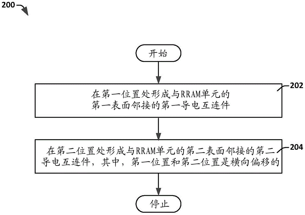
RRAM cell structure for beva/teva with lateral offset
A lateral offset, resistive random technology, applied in electrical components, semiconductor devices, circuits, etc., can solve problems such as high contact resistance change rate
- Summary
- Abstract
- Description
- Claims
- Application Information
AI Technical Summary
Problems solved by technology
Method used
Image

Examples
Embodiment Construction
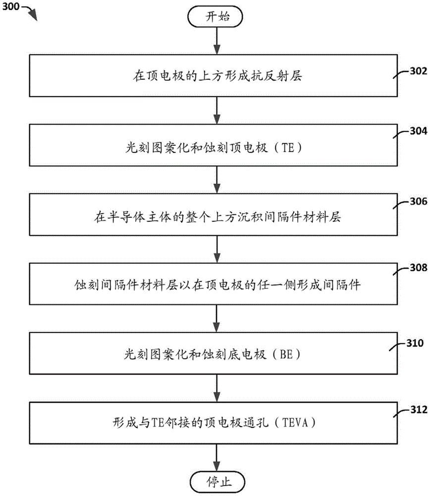
[0044] The description herein is made with reference to the drawings, wherein like reference numerals are generally used to refer to like elements throughout and the different structures are not necessarily drawn to scale. In the following description, for the purpose of illustration, numerous specific explanations are given for understanding. However, it will be apparent to those skilled in the art that one or more aspects herein may be practiced with a lesser degree of this detailed description. In other instances, well-known structures and devices are shown in block diagram form to facilitate understanding.
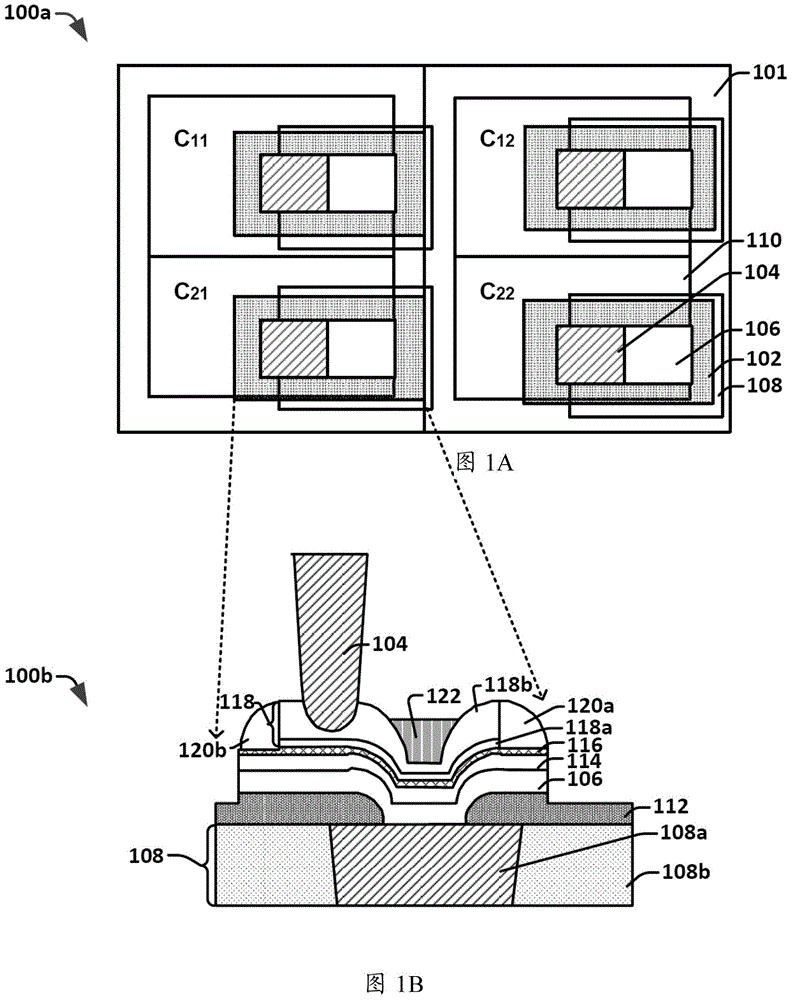
[0045]An RRAM cell includes two electrodes with a resistive switching element disposed between the two electrodes. The resistive switching element or variable resistive dielectric layer is prepared using a "forming process" to prepare the memory device for use. Typically the forming process is applied in a factory, assembly or initial system configuration. Resistive...
PUM
 Abstract
Description
Claims
Application Information
 - R&D
- Intellectual Property
- Life Sciences
- Materials
- Tech Scout
- Unparalleled Data Quality
- Higher Quality Content
- 60% Fewer Hallucinations
Browse by: Latest US Patents, China's latest patents, Technical Efficacy Thesaurus, Application Domain, Technology Topic, Popular Technical Reports.
© 2025 PatSnap. All rights reserved.Legal|Privacy policy|Modern Slavery Act Transparency Statement|Sitemap|About US| Contact US: help@patsnap.com