Packaging method of OLED (Organic Light Emitting Diode) and OLED packaging structure
An encapsulation method and encapsulation cover plate technology, which are applied in the direction of organic semiconductor devices, electrical components, electric solid devices, etc., can solve the problems of OLED device performance degradation, large molecular gap, and shortened lifespan, so as to improve performance and reduce oxygen and water vapor , the effect of prolonging the service life
- Summary
- Abstract
- Description
- Claims
- Application Information
AI Technical Summary
Problems solved by technology
Method used
Image

Examples
Embodiment approach 1
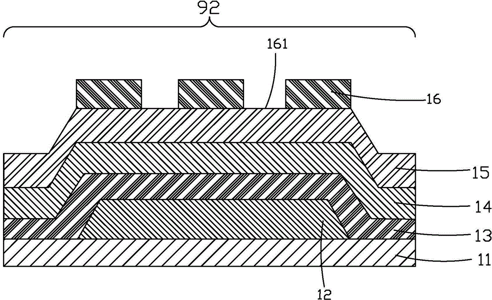
[0047] Such as image 3 As shown, a photoresist layer 16 is coated on the surface of the passivation protection layer 15 located in the packaging area 92, and several through holes 161 arranged at intervals are formed on the photoresist layer 16 through a photomask exposure and development process, so that The surface of the photoresist layer 16 becomes uneven, and in the subsequent packaging process, the contact area between the sealant 4 and the surface of the TFT substrate 1 can be increased, and finally the bonding force between the packaging cover plate 2 and the TFT substrate 1 can be improved;
[0048] Specifically, the thickness of the photoresist layer 16 , that is, the depth of the through hole 161 is 0-50 μm.
Embodiment approach 2
[0050] Such as Figure 4-5 As shown, a photoresist layer 16 is coated on the surface of the passivation protection layer 15 located in the encapsulation area 92, and the passivation protection layer 15 and the etching barrier are formed through the photomask exposure, development, etching and photoresist removal processes Several grooves 151 arranged at intervals are formed on the layer 14, and the grooves 151 penetrate the passivation protection layer 15 but do not penetrate the etching barrier layer 14, so that the passivation protection layer 15 and the etching A concave-convex surface is formed on the etching barrier layer 14, and in the subsequent packaging process, the contact area between the sealant 4 and the surface of the TFT substrate 1 can be increased, and finally the bonding force between the packaging cover plate 2 and the TFT substrate 1 can be improved;
[0051] Specifically, the depth of the groove 151 is 0-50 μm.
Embodiment approach 3
[0053] Such as Image 6 As shown, chemical vapor deposition (CVD) technology is used to form a rough inorganic layer 17 on the surface of the passivation protection layer 15 located in the packaging area 92 by controlling the parameters such as the temperature and voltage of the chemical vapor deposition, so that all The surface of the packaging area of the TFT substrate 1 becomes uneven. In the subsequent packaging process, the contact area between the sealant 4 and the surface of the TFT substrate 1 can be increased, and finally the bonding force between the packaging cover plate 2 and the TFT substrate 1 can be improved. ;
[0054] Preferably, the material of the inorganic layer 17 is silicon nitride (SiNx) or silicon dioxide (SiO 2 ).
[0055] Step 3, if Figure 7 As shown, the OLED device 3 is fabricated on the display area 91 of the TFT substrate 1 .
[0056] Step 4, providing the package cover plate 2, such as Figure 8 As shown, sealant 4 is coated on the surfac...
PUM
 Abstract
Description
Claims
Application Information
 - R&D
- Intellectual Property
- Life Sciences
- Materials
- Tech Scout
- Unparalleled Data Quality
- Higher Quality Content
- 60% Fewer Hallucinations
Browse by: Latest US Patents, China's latest patents, Technical Efficacy Thesaurus, Application Domain, Technology Topic, Popular Technical Reports.
© 2025 PatSnap. All rights reserved.Legal|Privacy policy|Modern Slavery Act Transparency Statement|Sitemap|About US| Contact US: help@patsnap.com