Multi-single-tube-semiconductor laser optical fiber coupling packaging device

A technology for fiber coupling and packaging devices, which is applied in the field of multi-single-tube semiconductor laser fiber coupling packaging devices, can solve the problems of increasing the number of rows, low material utilization rate, difficult manufacturing process, etc., and achieves the effect of increasing the number of

Inactive Publication Date: 2015-04-22
深圳凯普林光电科技有限公司
View PDF8 Cites 26 Cited by
  • Summary
  • Abstract
  • Description
  • Claims
  • Application Information

AI Technical Summary

Problems solved by technology

However, its function is also limited so that it can only combine two beams of light with vertical polarization states, which limits the increase in the number of rows of this product.
The number of chips in each row is also limited by the optical parameters and convergence characteristics of the converging lens 109 and cannot be increased indefinitely, so that it is difficult to break through 200 watts of products with this structure (20 semiconductor laser chip packages)
[0006] Because this kind of device 100 uses an integral metal casing as the carrier of semiconductor laser chips 101 and lenses, at first it is necessary to weld a plurality of semiconductor laser chips 101 into the ca

Method used


Image

  • Multi-single-tube-semiconductor laser optical fiber coupling packaging device
  • Multi-single-tube-semiconductor laser optical fiber coupling packaging device
  • Multi-single-tube-semiconductor laser optical fiber coupling packaging device

Examples


Embodiment Construction

[0030] In order to make the object, technical solution and advantages of the present invention clearer, the present invention will be further described in detail below in conjunction with the accompanying drawings and embodiments. It should be understood that the specific embodiments described here are only used to explain the present invention, not to limit the present invention.

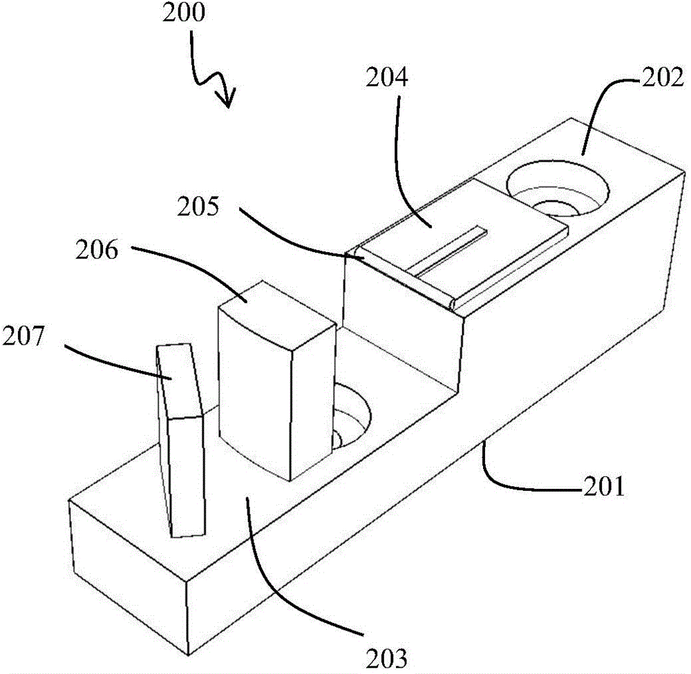
[0031] figure 2 It is a schematic structural diagram of the single-chip independent optical path module 200 of the present invention; figure 2 As shown, the single-chip independent optical path module 200 of the present invention includes a stepped carrier 201, which is long and made of metal. In the present invention, the length direction of the carrier 201 is defined as the first direction, that is, the carrier 201 extends along the first direction. The upper surface of the carrier 201 forms a first surface 202 and a second surface 203 with different heights, which are arranged side by side i...


PUM


Abstract

The invention provides a multi-single-tube-semiconductor laser optical fiber coupling packaging device. The device comprises at least one multi-step base, a plurality of single chip independent optical path modules, a fast axis convergent lens, a slow axis convergent lens and an optical fiber output end. The multi-step base comprises a plurality of step faces with the height increased sequentially. The single chip independent optical path modules are sequentially arranged on the multi-step base. Each single chip independent optical path module comprises a carrier, semiconductor laser chips, a fast axis collimating lens, a slow axis collimating lens and a reflector, wherein the semiconductor laser chips are sequentially fixed to the carrier in the first direction, the fast axis collimating lens and the slow axis collimating lens are used for collimating light beams emitted by the semiconductor laser chips, and the reflector is used for reflecting the collimated light beams. The fast axis convergent lens is used for converging light beams emitted by all the single chip independent optical path modules in the fast axis direction. The slow axis convergent lens is used for converging light beams emitted by all the single chip independent optical path modules in the slow axis direction. The optical fiber output end is used for coupling of the converged light beams. The single chip independent optical path modules are arranged on the multi-step base in the section direction.

Description

technical field [0001] The invention relates to a semiconductor laser device, more specifically, to a multi-single-tube semiconductor laser fiber coupling packaging device. Background technique [0002] Due to the structural characteristics and luminous characteristics of the semiconductor laser, the light emitted by it has a large divergence angle and a narrow light-emitting area in the direction perpendicular to the active layer (commonly known as the fast axis), and in the direction parallel to the active layer (commonly known as the slow axis). It has a smaller divergence angle and a larger luminous area. Due to the spatial divergence of the beam, if multiple semiconductor laser chips need to be packaged into a product with optical fiber output, it is necessary to first collimate the beams emitted by the semiconductor laser chips on the fast axis and slow axis beams, and shape the beams into An elliptical beam of approximately parallel light, and then perform optical de...

Claims


Application Information

Patent Timeline
IPC IPC(8): H01S5/40H01S5/06
Inventor 姜立国
Owner 深圳凯普林光电科技有限公司
Why Eureka
Try Eureka