Test structure and forming method thereof and testing method

A technology for testing structure and fixing structure, applied in microstructure technology, microstructure device, manufacturing microstructure device, etc., can solve the problems of complex test process and low test structure accuracy, and achieve a small test range, a relatively high test range, Test the effect of a simple structure

Active Publication Date: 2015-04-29
SEMICON MFG INT (SHANGHAI) CORP
View PDF9 Cites 0 Cited by
  • Summary
  • Abstract
  • Description
  • Claims
  • Application Information

AI Technical Summary

Problems solved by technology

[0005] However, when testing existing test structures with testing equipment for detecting three-dimensi

Method used


Image

  • Test structure and forming method thereof and testing method
  • Test structure and forming method thereof and testing method
  • Test structure and forming method thereof and testing method

Examples


Embodiment Construction

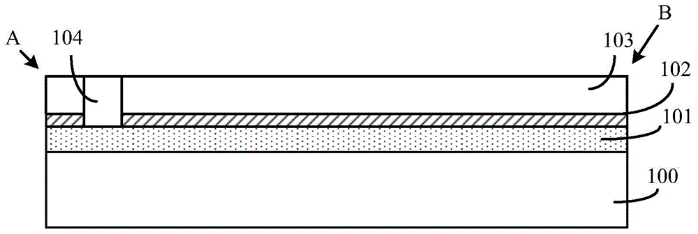
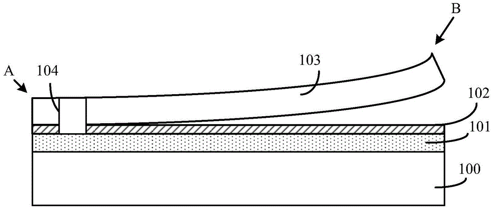
[0039] As mentioned in the background, when using the test equipment for detecting three-dimensional structures to test the existing test structure, the test process is complicated, and the accuracy of the obtained test structure is low.

[0040] Please refer to figure 1 , figure 1 It is a schematic diagram of a test structure embodiment, including: a substrate 100; a dielectric layer 101 located on the surface of the substrate 100; a sacrificial layer 102 located on the surface of the dielectric layer 101; a stress layer 103 located on the surface of the sacrificial layer 102, and the sacrificial layer There is a lattice mismatch between the material of the stress layer 102 and the material of the stress layer 103, so that the surface of the stress layer 103 in contact with the sacrificial layer 102 is subjected to stress, and the A end of the stress layer 103 has a and a sacrificial layer 102 , and a plug 104 extending into the dielectric layer 101 , the plug 104 fixes the ...


PUM


Abstract

The invention discloses a test structure and a forming method thereof and a testing method, wherein the test structure comprises a medium layer, a first sacrificial layer, a bending layer, a fixing structure, a first opening, and a second plug, wherein the medium layer is positioned on the surface of a substrate; the first sacrificial layer is positioned on the surface of the medium layer; the bending layer is positioned on the surface of the first sacrificial layer; the bending layer and the first sacrificial layer are made from different materials, and the contact surface of the bending layer and the first sacrificial layer has stress; the fixing structure is positioned on the first end of the bending layer, and comprises a first plug which penetrates through the bending layer and the first sacrificial layer and is positioned on the surface of the medium layer; the first opening surrounds the fixing structure; the graph on the top of the first opening is annular; the first opening is exposed out of the side surface of the fixing structure and the surface of the first sacrificial layer; the second plug is positioned on the second end of the bending layer, penetrates through the bending layer and the first sacrificial layer and is positioned on the surface of the medium layer, and the second end is opposite to the first end; the material of the fixing structure or the second plug is different from that of the first sacrificial layer. The process for testing by adopting the test structure is simple, and the accuracy is high.

Description

technical field [0001] The invention relates to the technical field of semiconductor manufacturing, in particular to a test structure, its forming method, and a test method. Background technique [0002] Micro-Electro Mechanical System (MEMS for short) is an integrated device that acquires information, processes information and performs operations. Sensors in MEMS can receive external information such as pressure, position, velocity, acceleration, magnetic field, temperature or humidity, and convert the obtained external information into electrical signals for processing in MEMS. [0003] Most of the existing MEMS devices are three-dimensional (3D, 3-Dimensional) structures. Taking a capacitive pressure sensor in an existing MEMS device as an example, the capacitive pressure sensor includes a first electrode layer; a second electrode layer positioned on the surface of the first electrode layer, the first electrode layer and the second electrode layer The electrode layers a...

Claims


Application Information

Patent Timeline
IPC IPC(8): B81C1/00B81B7/00G01D5/12G01B7/28
Inventor 郑超骆凯玲
Owner SEMICON MFG INT (SHANGHAI) CORP
Why Eureka
Try Eureka