

A surface plasmon propagation device with full compensation of graphene waveguide excited by periodic diffraction folds
A technology of surface plasmon and graphene, which is applied in the field of optical communication, can solve problems such as the application of photon loop optical communication that cannot be realized
- Summary
- Abstract
- Description
- Claims
- Application Information
AI Technical Summary
Problems solved by technology
Method used
Image

Examples
Embodiment
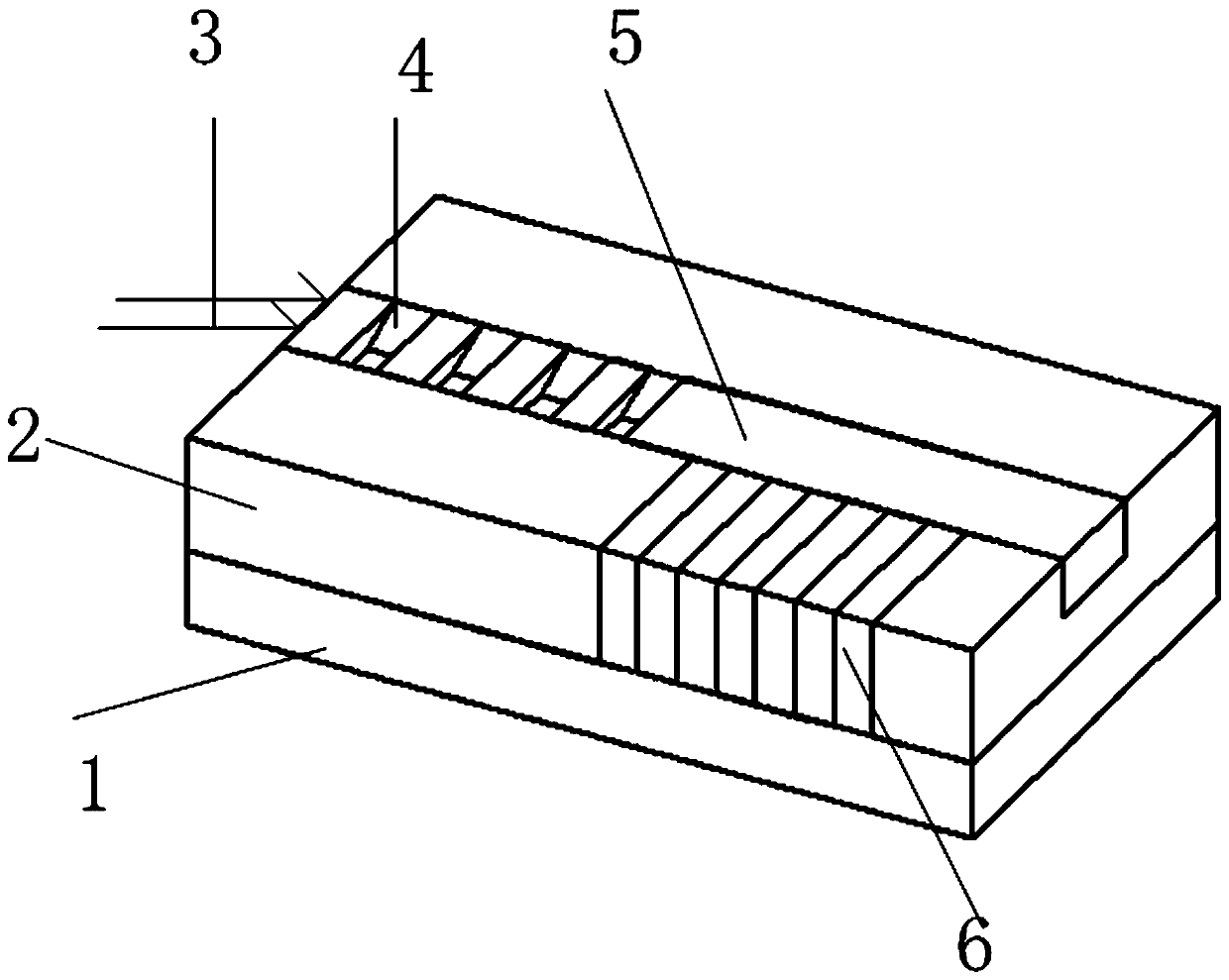
[0019] Reference figure 1 , A graphene waveguide full compensation surface plasmon propagation device excited by periodic diffraction folds, comprising a Si substrate 1 and SiO oxidized by the Si substrate 2 Dielectric layer 2, in SiO 2 The surface of the dielectric layer 2 is provided with a graphene waveguide 5 for propagating surface plasmons. One end of the graphene waveguide 5 is etched with a wrinkle structure 4 for exciting SPPs, and the other end of the graphene waveguide 5 is SiO 2 The dielectric layer 2 is filled with a dye gain medium 6.
[0020] SiO 2 The dielectric layer 2 is formed by the Si substrate 1 in an oxygen environment, and has a thickness of 800 nm.
[0021] The graphene waveguide 5 is a graphene strip waveguide.
[0022] The graphene strip waveguide is in SiO 2 The dielectric layer 2 adopts an electron beam exposure mask method to etch and etch a graphene strip waveguide with a depth of 600 nm.
[0023] The dye gain medium 6 is a dye gain medium with a periodi...
PUM
 Abstract
Description
Claims
Application Information