Check patentability & draft patents in minutes with Patsnap Eureka AI!

LDMOS (laterally diffused metal oxide semiconductor) and manufacture method thereof

A manufacturing method and metal technology, applied in semiconductor/solid-state device manufacturing, electrical components, circuits, etc., can solve the problem of reducing the number of devices, and achieve the effect of increasing the breakdown voltage

Active Publication Date: 2015-04-29
SEMICON MFG INT (SHANGHAI) CORP
View PDF6 Cites 4 Cited by
  • Summary
  • Abstract
  • Description
  • Claims
  • Application Information

AI Technical Summary

Problems solved by technology

An existing method to increase the breakdown voltage of LDNMOS is to expand the area of ​​​​the N-drift region, which will lead to a reduction in the number of devices per unit area

Method used


Image

  • LDMOS (laterally diffused metal oxide semiconductor) and manufacture method thereof
  • LDMOS (laterally diffused metal oxide semiconductor) and manufacture method thereof
  • LDMOS (laterally diffused metal oxide semiconductor) and manufacture method thereof

Examples


Embodiment Construction

[0036] In order to make the object, technical solution, and advantages of the present invention clearer, the present invention will be further described in detail below with reference to the accompanying drawings and examples.

[0037] The present invention has been described in detail using schematic diagrams. When describing the embodiments of the present invention in detail, for the convenience of explanation, the schematic diagram showing the structure will not be partially enlarged according to the general scale, which should not be used as a limitation of the present invention. In addition, in actual production In , the three-dimensional space dimensions of length, width and depth should be included.

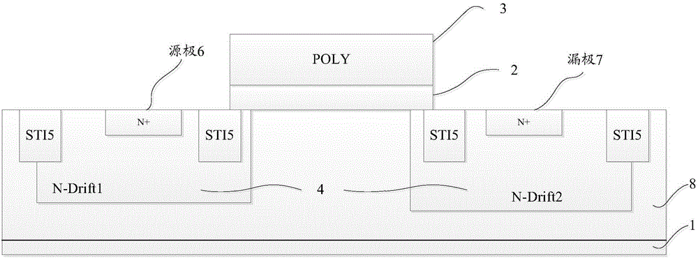
[0038] The method of the present invention is applicable to LDNMOS and LDPMOS.

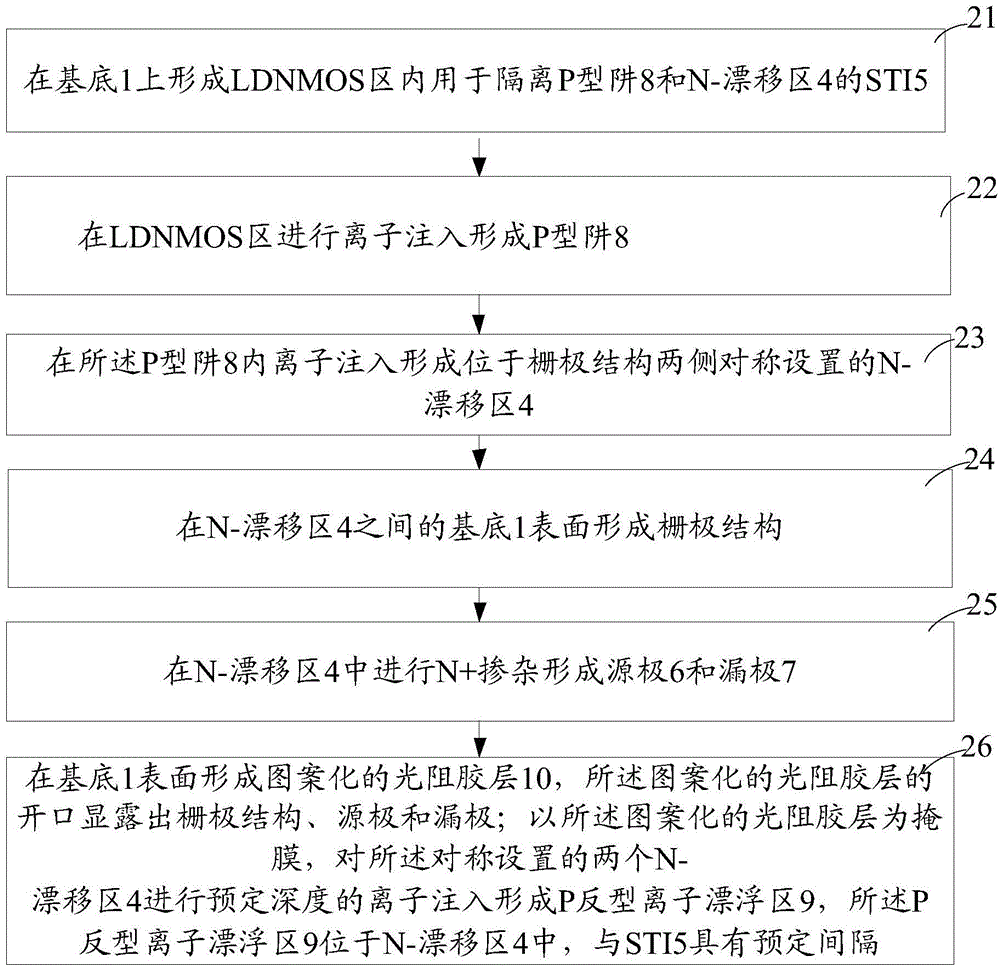
[0039] A schematic flow chart of the LDNMOS manufacturing method in a preferred embodiment of the present invention is as follows figure 2 As shown, it includes the following steps, which ar...


PUM


Abstract

The invention provides an LDMOS (laterally diffused metal oxide semiconductor) and a manufacture method thereof. The LDMOS is an LDNMOS. The method comprises the following steps: an STI, a P-shaped trap, two N-drift regions, a grid electrode structure, a source electrode and a drain electrode are sequentially formed on a base; a patterned light resistance adhesive layer is formed on the surface of the base after the grid electrode structure is formed; the opening of the patterned light resistance adhesive layer is exposed to the grid structure, the source electrode and the drain electrode; the patterned light resistance adhesive layer adopts a mask; ion implantation at predetermined depth is performed on the two symmetrically arranged N-drift regions, so as to form a P reversed ion floating region; the P reversed ion floating region is positioned in the N-drift regions and forms a predetermined distance with the STI. The invention further provides an LDMOS and a manufacture method thereof. The LDMOS is an LDNMOS. By adopting the LDMOS, breakdown voltage can be improved.

Description

technical field [0001] The invention relates to the field of semiconductor devices and their manufacture, in particular to an LDMOS (Laterally Diffused Metal Oxide Semiconductor Transistor) and a manufacturing method thereof. Background technique [0002] Laterally Diffused Metal Oxide Semiconductor (LDMOS) is mainly used in power integrated circuits, such as RF power amplifiers for mobile phone base stations, and can also be used in high frequency, UHF and UHF broadcast transmitters And microwave radar and navigation systems. LDMOS technology brings higher power peak-to-average ratio, higher gain and linearity to the new generation of base station amplifiers, and at the same time brings higher data transmission rates to multimedia services. [0003] The structure of the existing laterally diffused N type metal oxide semiconductor transistor (Laterally Diffused N type Metal Oxide semiconductor, LDNMOS) is as follows figure 1 As shown, the LDNMOS has a substrate 1 on which ...

Claims


Application Information

Patent Timeline
Patent Type & Authority Applications(China)
IPC IPC(8): H01L21/336H01L29/78H01L29/06
CPCH01L29/0603H01L29/0684H01L29/66681H01L29/7816
Inventor 黄晨
Owner SEMICON MFG INT (SHANGHAI) CORP
Features
  • R&D
  • Intellectual Property
  • Life Sciences
  • Materials
  • Tech Scout
  • Unparalleled Data Quality
  • Higher Quality Content
  • 60% Fewer Hallucinations
Learn More