Method for improving indium thermal conductive interface material

An interface material and material strip technology, which is applied in the field of improving the thermal conductivity of indium interface materials, can solve the problems of easy residual thermal stress and low thermal conductivity.

Active Publication Date: 2015-05-06
SOLDERWELL MICROELECTRONIC PACKAGING MATERIALS CO LTD
View PDF4 Cites 1 Cited by
  • Summary
  • Abstract
  • Description
  • Claims
  • Application Information

AI Technical Summary

Problems solved by technology

Traditional phase-change thermal interface materials mainly refer to thermoplastic resins whose melting temperature is generally 50-80°C, but these thermoplastic resins themselves have very low thermal conductivity.
Another type of phase change thermal interface material - low melting point metals, but it is easy to retain thermal stress when it changes from liquid to solid

Method used


Image

  • Method for improving indium thermal conductive interface material
  • Method for improving indium thermal conductive interface material

Examples


Embodiment Construction

[0031] The following examples are further detailed descriptions of the present invention.

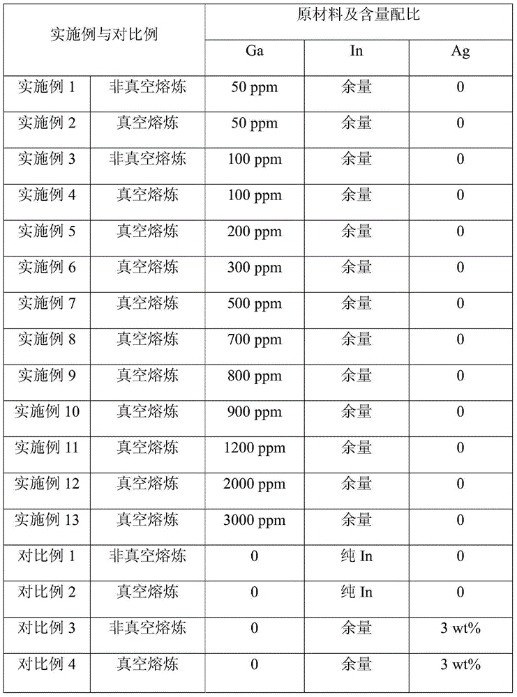
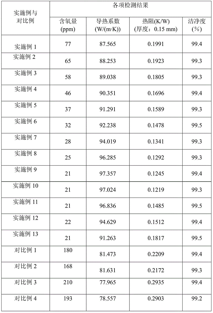
[0032] The method for improving the indium thermal interface material provided by the present invention is mainly reflected in adding 50-3000 ppm gallium to pure indium during the smelting process.

[0033] The technological process of this embodiment is:

[0034] 1. Special smelting process, put the pre-prepared pure indium in a vacuum induction melting furnace, first melt it at 280-320°C under non-vacuum conditions, and add 50-3000ppm gallium to the melted pure indium, stir 2 to 3 minutes and thoroughly remove the slag, then close the furnace cover, wait for the vacuum to be below 10Pa and keep it for half an hour, then cast into ingots under vacuum conditions, and remove the rough skin;

[0035] 2. Extrusion process, extruding the stripped ingot on the extruder to form a billet;

[0036] 3. Rolling process, rolling the strip blank on the rolling mill into a strip of required thickn...


PUM


Abstract

The invention discloses a method for improving an indium thermal conductive interface material and belongs to the technical field of thermal conductive interface materials. The method aims at solving the problems of high density and heat dissipation of ultra-large scale integrated circuits. The method for improving the indium thermal conductive interface material is mainly characterized in that 50-3000ppm gallium is added in pure indium during the smelting process. The thermal conductive interface material obtained by the method has the advantages of no toxicity, no harm, high thermal conductivity, high flexibility, easiness in installation and dismountability and the surface cleanliness of obtained thermal conductive interface material reaches above 90% and the oxygen content is below 25ppm.

Description

technical field [0001] The invention relates to the technical field of thermally conductive interface materials, in particular to a method for improving indium thermally conductive interface materials. Background technique [0002] With the increasing miniaturization and miniaturization of electronic components, integrated circuits (chips) with ultra-high density and ultra-large scale will be the general trend of integrated circuits in the future. The increase in integration and power consumption density will inevitably lead to an increase in the heat density of integrated circuits and electronic devices during operation, thereby increasing the temperature during operation. Therefore, the heat dissipation problem of electronic packaging is becoming more and more important for the working efficiency and reliability of electronic devices. Especially those high-power consumption devices, such as high-power diode lasers, high-brightness light-emitting diodes and high-power senso...

Claims


Application Information

Patent Timeline
IPC IPC(8): C22C28/00C22C1/02
Inventor 蔡航伟胡鸿杜昆蔡烈松陈明汉
Owner SOLDERWELL MICROELECTRONIC PACKAGING MATERIALS CO LTD
Why Eureka
Try Eureka