Manufacturing method for interconnected through holes in wafer level chip size packaging

A wafer-level chip and size packaging technology, which is applied in semiconductor/solid-state device manufacturing, electrical components, circuits, etc., can solve problems that affect the reliability of packaged chips, circuit short circuits, complex process steps, etc., and achieve simple methods and improve reliability. performance, the effect of simple encapsulation steps

Active Publication Date: 2015-05-13
HUATIAN TECH KUNSHAN ELECTRONICS
View PDF4 Cites 21 Cited by
  • Summary
  • Abstract
  • Description
  • Claims
  • Application Information

AI Technical Summary

Problems solved by technology

In the above etching method, after the opening is formed, the dielectric layer on the pad must be removed by etching first, and then the insulating layer is laid. The thickness of the two layers of material is greater than the thickness of the insulating layer on the back of the wafer. There will be a phenomenon that the insulating layer on the plane is etched away before the pad is exposed. If the insulating layer on the plane is too thin or there is no insulating layer, the subsequent packaging process will cause a short circuit in the
Affects the reliability of packaged chips, and the process steps are more complicated

Method used


Image

  • Manufacturing method for interconnected through holes in wafer level chip size packaging
  • Manufacturing method for interconnected through holes in wafer level chip size packaging
  • Manufacturing method for interconnected through holes in wafer level chip size packaging

Examples


Embodiment 1

[0044] Such as figure 1 , figure 2 , image 3 , Figure 4 , Figure 5 , Figure 6 , Figure 7 , Figure 8 and Figure 9 As shown, a method for manufacturing through-hole interconnection in a wafer-level chip size package, comprising the following steps:

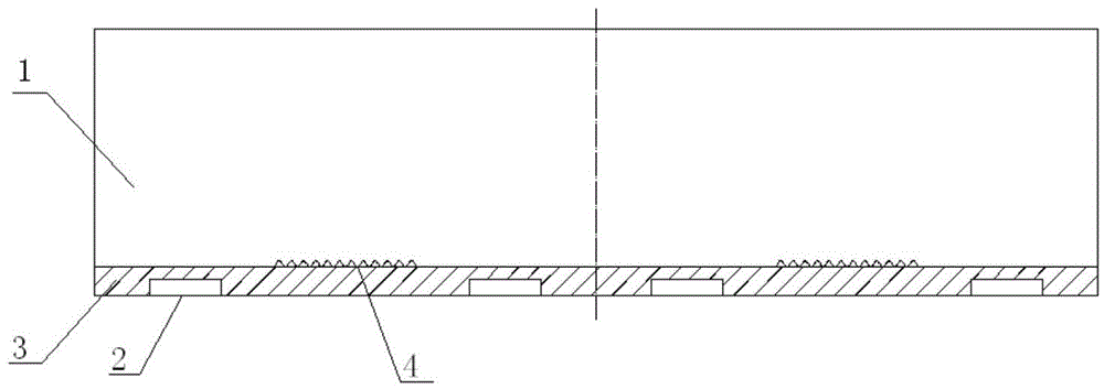
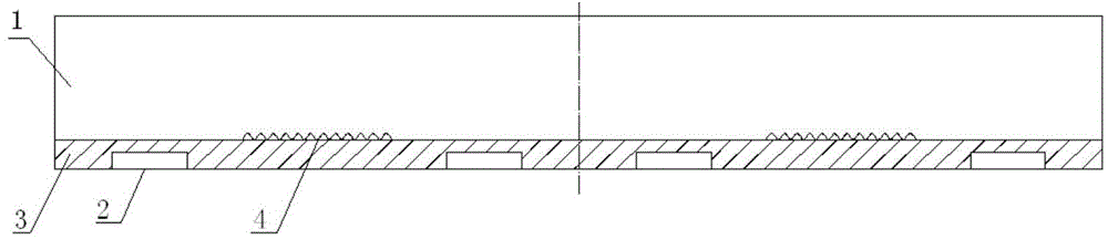
[0045] a. see figure 1 , provide a wafer with several chip units, the chip unit includes a base 1 and a dielectric layer 3 on the front side of the base 1, the front side of the base 1 is provided with an element area 4, and the periphery of the element area 4 A plurality of welding pads 2 are provided, and the welding pads 2 are located in the dielectric layer 3, and the element area 4 is electrically connected to the surrounding welding pads 2;

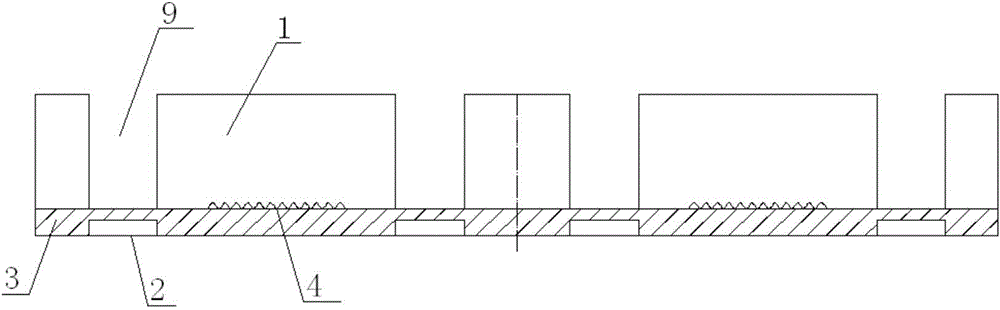
[0046] b. see image 3 A first opening 9 opposite to the welding pad 2 is formed on the back of the substrate 1, and the first opening 9 extends from the back of the substrate 1 to above the corresponding welding pad 2, and exposes the welding pad 2, that is, there is a...

Embodiment 2

[0062] Such as Figure 10 and Figure 11 As shown, this embodiment 2 includes all the technical features in the above embodiment 1, the difference is that step b is replaced by: forming a first opening 9 opposite to the welding pad 2 on the back of the substrate 1, and the The first opening 9 extends from the back of the substrate 1 to above the corresponding pad 2 and exposes the surface of the pad 2 . Step d is replaced by: removing the photoresist layer 5 above the welding pad 2 through a photolithography process to expose the surface of the welding pad 2 . That is, according to the extent to which the first opening 9 extends toward the back of the substrate 1 , the barrier material on the pad 2 may include the material of the photoresist layer 5 or a combination of the material of the dielectric layer 3 and the material of the photoresist layer 5 . For example, when the surface of the welding pad 2 is exposed, the barrier material on the welding pad 2 is only the photore...


PUM


Abstract

The invention discloses a manufacturing method for interconnected through holes in wafer level chip size packaging. The method comprises the steps of removing stopping materials on a welding pad by the etching method; paving photoresist in the whole opening and on the rear surface of a substrate so as to form a photoresist layer; exposing and developing to remove the photoresist layer above the welding pad; removing a dielectric layer above the welding pad by the dry etching method. The method is simple and easy to be carried out; in addition, the dielectric layer on the welding pad is removed by dry etching, and thus problem that the upper dielectric layer on the welding pad is not etched but is completely removed, and an insulating layer on the rear surface of a wafer is etched to be thin or completely used to lead to short circuit of a line can be avoided. With the adoption of the method, the process of forming silicon through hole interconnection by the etching method can be simplified; the wafer level chip size packaging is simplified; therefore, the packaging efficiency is increased, and meanwhile, the packaging reliability is improved.

Description

technical field [0001] The invention relates to wafer-level chip size packaging, in particular to a method for making through-hole interconnections in wafer-level chip size packaging. Background technique [0002] The popularization of portable consumer electronic products and consumers' demand for such products has made the function and high integration of IC chips more and more demanding. In order to meet this requirement, the package size is required to be light, thin and short, and the transmission speed is increased. Therefore, it is often necessary to form a vertical through-silicon via interconnection structure. [0003] The existing packaging method adopts wafer-level chip size packaging, and the general structure of the wafer is as follows: figure 1 As shown, the wafer includes several chip units, and each chip unit includes a base 1 and a dielectric layer 3 located on the front side of the base. The front side of the base is provided with an element area 4, and se...

Claims


Application Information

Patent Timeline
Patent Type & Authority Applications(China)
IPC IPC(8): H01L21/768
CPCH01L21/768H01L23/522
Inventor 范俊黄小花沈建树王晔晔钱静娴翟玲玲
Owner HUATIAN TECH KUNSHAN ELECTRONICS
Why Eureka
Try Eureka