Printed circuit board (PCB) manufacturing method

A technology of PCB board and manufacturing method, which is applied in the direction of improving the metal adhesion of insulating substrates, removing conductive materials by chemical/electrolytic methods, and manufacturing printed circuits. Fix problems such as poor bonding identification, achieve the effects of reducing burrs and side etching, good flatness, and improving etching effects

Active Publication Date: 2015-05-13
HUIZHOU XINGZHIGUANG TECH
View PDF4 Cites 7 Cited by
  • Summary
  • Abstract
  • Description
  • Claims
  • Application Information

AI Technical Summary

Problems solved by technology

The surface flatness of the PCB produced by the traditional PCB board production process is not enough, the color is dull, the bonding identification is poor, the bonding is desoldered, the bonding is offset, and the bonding tension value is small, which affects the quality of the PCB board

Method used


Image

  • Printed circuit board (PCB) manufacturing method
  • Printed circuit board (PCB) manufacturing method
  • Printed circuit board (PCB) manufacturing method

Examples


Embodiment

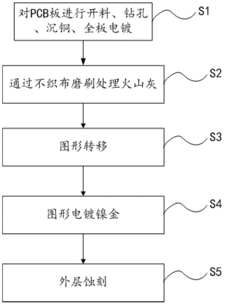
[0037] Such as figure 1 Shown, a kind of manufacturing method of PCB board comprises the following steps:

[0038] S1 performs material cutting, drilling, copper sinking, and full board electroplating on the PCB. The specific process is as follows:

[0039] S101 Cutting materials to form a jigsaw panel, which includes an inner layer substrate and an inner layer copper foil attached to the upper and lower surfaces of the inner layer substrate.

[0040] S102 Drilling, drilling the required holes on the PCB to form a conductive channel between the connecting lines.

[0041] S103 sinking copper, using the principle of chemical reaction to deposit a layer of 0.3um-0.5um copper on the hole wall, so that the originally insulated hole wall has conductivity, which facilitates the smooth progress of subsequent PCB surface plating and pattern plating, thus completing Electrical intercommunication between PCB board circuit networks.

[0042] S104 full board electroplating, protecting ...


PUM


Abstract

The invention relates to a PCB manufacturing method. The method comprises the steps of S1, performing cutting, drilling, electroless copper plating and full-board electroplating; S2, brushing and processing cinerite through non-woven fabrics; S3, pattern transfer; S4, pattern nickel gold electroplating; S5, outer layer etching. By the aid of the method, the PCB bonding tension value can reach 9N, compared with the prior art, the bonding tension value is improved greatly, the problems of bonding de-soldering, bonding deviation, poor bonding recognition and the like are solved effectively, and accordingly, the PCB quality is improved greatly.

Description

technical field [0001] The invention relates to the technical field of PCB board production, in particular to a method for manufacturing a PCB board. Background technique [0002] PCB (Printed Circuit Board), printed circuit board, also known as printed circuit board, printed circuit board, is a support for electronic components. PCB board: the insulating board is used as the base material, cut to a certain size, with at least one conductive pattern on it, and holes (such as component holes, fastening holes, metallized holes, etc.), used to replace the electronic components of the previous device The chassis of the device and realize the interconnection between electronic components. Since such boards are made using electronic printing, they are called "printed" circuit boards. [0003] The traditional PCB board production process includes: material cutting—drilling—copper sinking—full board plating—graphic transfer—graphic copper nickel gold plating—outer layer etching—ou...

Claims


Application Information

Patent Timeline
Patent Type & Authority Applications(China)
IPC IPC(8): H05K3/00
CPCH05K3/06H05K3/26H05K3/38H05K2203/072
Inventor 闫红生杨科冯成庚
Owner HUIZHOU XINGZHIGUANG TECH
Why Eureka
Try Eureka