Semiconductor element

A technology for semiconductors and components, applied in the field of semiconductor components, can solve problems such as component damage, and achieve the effect of improving damage tolerance

Inactive Publication Date: 2015-05-13
FUJI ELECTRIC CO LTD
View PDF7 Cites 6 Cited by
  • Summary
  • Abstract
  • Description
  • Claims
  • Application Information

AI Technical Summary

Problems solved by technology

In addition, if the leakage current becomes too large in the off state, there is a problem of element destruction due to thermal runaway

Method used


Image

  • Semiconductor element
  • Semiconductor element
  • Semiconductor element

Examples


Embodiment approach 1

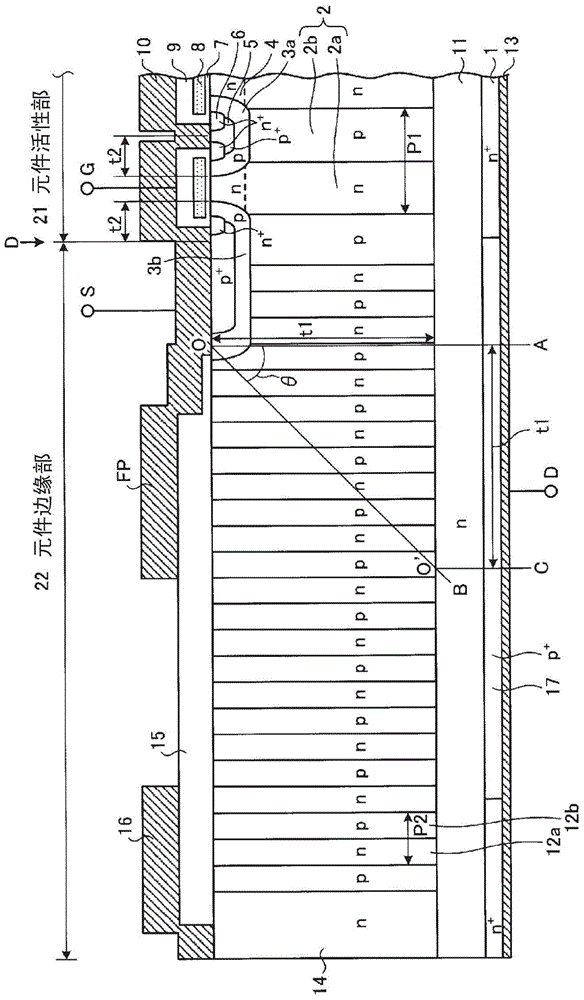
[0041] Taking an n-channel vertical MOSFET with a planar gate structure as an example, the semiconductor device structure described in Embodiment 1 will be described. figure 1 It is a cross-sectional view showing the structure of the semiconductor device according to the first embodiment. figure 1 The semiconductor element described in the illustrated embodiment 1 is a super-junction MOSFET provided with a drain drift portion (vertical drift portion) 2 of a first parallel pn structure. On the surface layer on one of the surface sides of the drain drift portion 2 (hereinafter referred to as the substrate surface side), a p base region 3a of high impurity concentration as the element active portion 21 is selectively provided. The substrate refers to an epitaxial substrate described later.

[0042] On the inner substrate surface side of the p base region 3a is selectively provided with high impurity concentration p + Contact area 5 and n + Source area 6. n + The source region 6 is...

Embodiment approach 2

[0067] The structure of the super junction semiconductor element described in Embodiment 2 will be described. figure 2 It is a cross-sectional view showing the structure of the semiconductor device according to the second embodiment. The difference between the super junction semiconductor element described in the second embodiment and the super junction semiconductor element described in the first embodiment is that an n-type bulk (BULK) region 31 continuous with the first parallel pn structure is provided instead of the second parallel pn structure. In addition, a p-type RESURF region 32 is provided on the surface layer on the substrate surface side of the n-type bulk region 31.

[0068] The n-type block region 31 is a region between the first parallel pn structure provided from the element active portion 21 to the element edge portion 22 and the n-type channel cutoff region 14 provided on the outermost side of the element edge portion 22. The p-type RESURF region 32 is selecti...

Embodiment approach 3

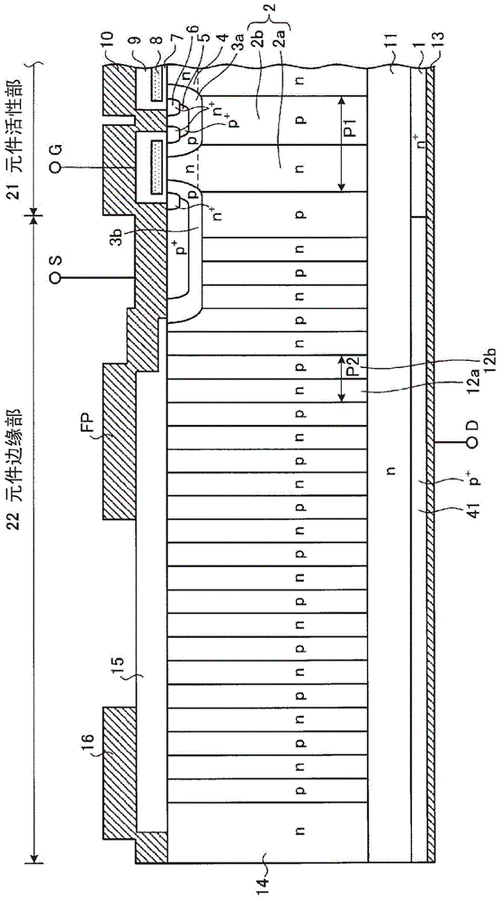
[0072] The structure of the super junction semiconductor element described in Embodiment 3 will be described. image 3 It is a cross-sectional view showing the structure of the semiconductor device according to the third embodiment. The difference between the super junction semiconductor element described in Embodiment 3 and the super junction semiconductor element described in Embodiment 1 is as follows: + The outer end portion of the drain region 41 extends to the outer periphery (the side surface of the substrate) of the element edge portion 22. The structure of the super junction semiconductor element described in Embodiment 3 other than this is the same as that of the super junction semiconductor element described in Embodiment 1. In addition to the p of the method of manufacturing a super junction MOSFET described in Embodiment 3 + Except for the difference in the formation range of the drain region 41, the other is the same as the manufacturing method of the super junctio...


PUM


Abstract

A drain / drift section (2) is generally equivalent to a portion directly below a p-base region (3a) which is an element active section (21), and is a first parallel pn structure obtained by repeatedly joining in an alternating manner a first n-type region (2a) and a first p-type region (2b). Around the drain / drift section (2) is an element peripheral edge section (22) comprising a second parallel pn structure obtained by repeatedly joining in an alternating manner a second n-type region (12a) and a second p-type region (12b) oriented continuous with the first parallel pn structure. An n-buffer layer (11) is provided between the first and second parallel pn structures and an n+ drain layer (1). A p+ drain region (17) is selectively provided on the interior of the n+ drain layer (1) of the element peripheral edge section (22), the p+ drain region (17) passing through the n+ drain layer (1) in the depth direction. By this means, damage resistance can be improved in a super-junction semiconductor element capable of significantly improving the tradeoff relationship between on resistance and pressure resistance.

Description

Technical field [0001] The present invention relates to a semiconductor element. Background technique [0002] Generally, semiconductor elements can be classified into horizontal semiconductor elements having electrodes on one side and vertical semiconductor elements having electrodes on both sides. The flowing direction of the drift current in the on state of the vertical semiconductor element is the same as the extension direction of the depletion layer formed by the reverse bias voltage in the off state. For example, in the n-channel vertical MOSFET (MOSFET: Metal Oxide Semiconductor Field Effect Transistor: MOS field effect transistor) of a common planar gate structure, the high resistance n - The drift layer part functions as a region in which drift current flows in the longitudinal direction in the on state. Therefore, if n - The current path of the drift layer is shortened, the drift resistance becomes lower, so the effect of reducing the actual on-resistance of the MOSFE...

Claims


Application Information

Patent Timeline
Patent Type & Authority Applications(China)
IPC IPC(8): H01L29/78H01L29/739
CPCH01L29/7811H01L21/263H01L21/26506H01L29/063H01L29/0634H01L29/0638H01L29/1095H01L29/402H01L29/739H01L29/78
Inventor 大西泰彦
Owner FUJI ELECTRIC CO LTD
Why Eureka
Try Eureka