Quad flat no-lead package lead frame structure and package structure

A square flat, leadless technology, applied in the direction of electrical solid devices, semiconductor devices, semiconductor/solid device components, etc., can solve the problems of loss of cutting tool life, gas escape, poor bonding of solder paste, etc., to achieve Reduce wear, improve cutting efficiency, and reduce metal thickness

Active Publication Date: 2015-05-27
JCET GROUP CO LTD
View PDF4 Cites 8 Cited by
  • Summary
  • Abstract
  • Description
  • Claims
  • Application Information

AI Technical Summary

Problems solved by technology

[0003] When the exposed pad and electrode contacts on the bottom of the chip are soldered to the hot pad on the PCB, there will be gas escape and the solder paste will not bond well
[0004] In addition, traditional QFN pins are cut and shaped, such as figure 1 As shown, since the pins are all made of solid metal, it is easy to consume the life of the cutting tool. Therefore, how to reduce the wear of the cutting tool is also a problem

Method used


Image

  • Quad flat no-lead package lead frame structure and package structure
  • Quad flat no-lead package lead frame structure and package structure
  • Quad flat no-lead package lead frame structure and package structure

Examples


Embodiment Construction

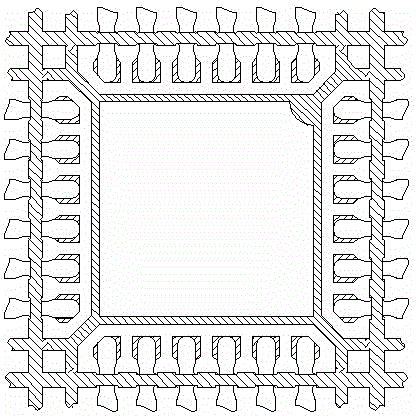
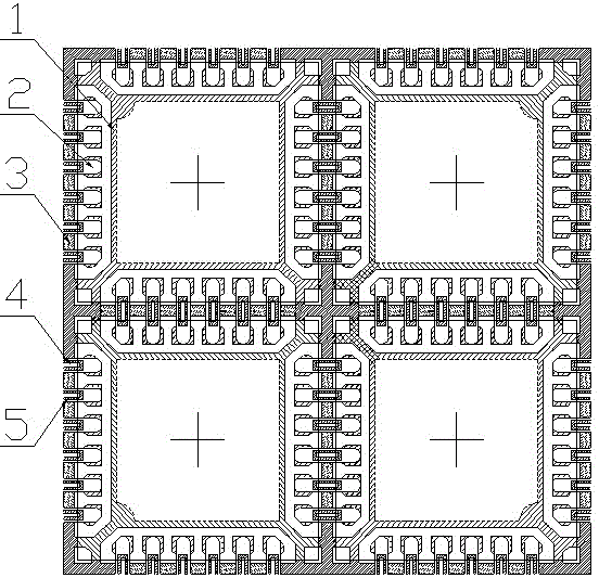
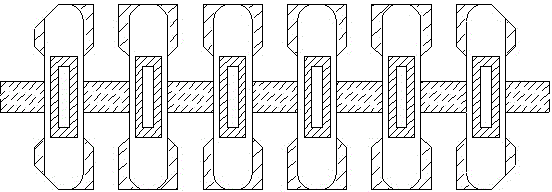
[0028] see figure 2 , the lead frame structure of the present invention is a quadrilateral flat no-lead type package, which includes several carrying units arranged in a matrix and middle ribs 3 for fixing the carrying units between the carrying units, the carrying units include chips The seat 1 and the pin array 2 arranged around the chip seat 1, the middle rib 3 is connected between the pin arrays 2 of two adjacent carrying units, and the back of the pin array 2 is provided with bumps near the middle rib 3 4. The bump 4 is rectangular, and a half-etched groove 5 is arranged around the rectangular bump 4. The bump 4 and the half-etched groove 5 are drawn around the half-etched bump on the back of the pin array near the middle rib. Formed by the pin and the middle rib, the bump 4 will still be partially retained after the rib is removed. The width of the retained part of the bump 4 is 1 / 4~1 / 2 of the width of the pin, and the length extends to 1 / 6~1 / 4, the depth of the half-e...


PUM


Abstract

The invention relates to a quad flat no-lead package lead frame structure. The quad flat no-lead package lead frame structure comprises a plurality of bearing units in matrix arrangement and middle glutens (3) arranged between and used for fixing the bearing units, wherein each bearing unit comprises a chip carrier (1) and a pin array (2) arranged at the periphery of the chip carrier; each middle gluten (3) is connected between the pin arrays (2) of two adjacent bearing units of the bearing units; a half-etched groove (4) is formed in the back, close to the corresponding middle gluten (3) , of each of the pin arrays (2). According to the quad flat no-lead package lead frame structure, as the half-etched grooves are formed in the root parts of pins, during applying of solder paste to a PCB, the solder paste can more successfully climb to the side edges of the pins through the siphonic effect, and accordingly, combination of the pins and the PCB is enhanced; as the half-etched grooves are formed in the root parts of the pins, the thickness of metal at the root parts of the pins is reduced, accordingly, tool abrasion is reduced and the quad flat no-lead cutting efficiency is greatly improved.

Description

technical field [0001] The invention relates to a lead frame structure and a package body structure of a square flat leadless type package, belonging to the technical field of semiconductor packaging. Background technique [0002] The quad flat no-lead package is one of the surface-mount packages. The quad flat no-lead package is square or rectangular. There is one or more exposed pads at the center of the bottom of the package for heat conduction. The four sides of the package are configured There are electrode contacts. [0003] When the exposed pad and electrode contacts on the bottom of the chip are soldered to the thermal pad on the PCB, gas will escape and cause poor bonding of the solder paste. [0004] In addition, traditional QFN pins are cut and shaped, such as figure 1 As shown, since the pins are all made of solid metal, it is easy to consume the life of the cutting tool. Therefore, how to reduce the wear of the cutting tool is also a problem. Contents of the...

Claims


Application Information

Patent Timeline
Patent Type & Authority Applications(China)
IPC IPC(8): H01L23/495H01L23/31
CPCH01L2224/97
Inventor 刘恺王亚琴王孙艳梁志忠
Owner JCET GROUP CO LTD
Why Eureka
Try Eureka