Preparation method for patterned organic thin film
A technology of organic thin film and organic thin film layer, which is applied in the field of preparation of patterned organic thin film, can solve problems such as thermal damage of non-processed layer, achieve the effects of reducing processing cost, easy guarantee of processing quality, and wide adjustment range
- Summary
- Abstract
- Description
- Claims
- Application Information
AI Technical Summary
Problems solved by technology
Method used
Image

Examples
preparation example Construction
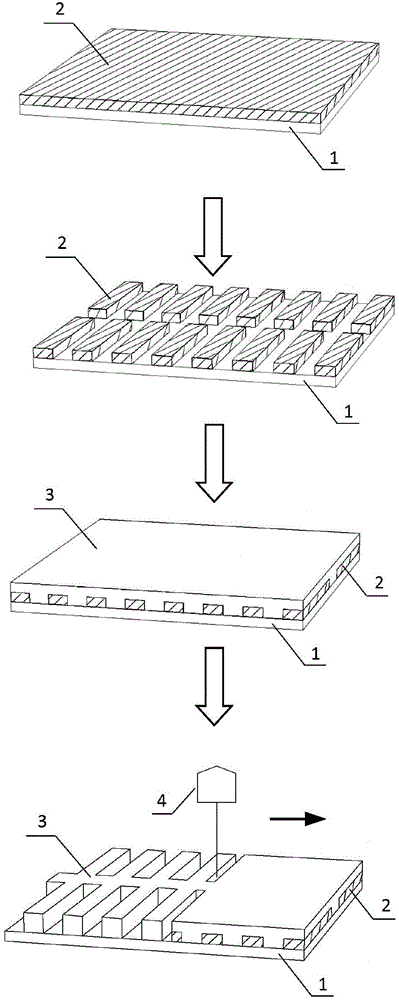
[0024] like figure 1 Shown, the preparation method of patterned organic thin film comprises the following steps:
[0025] Step 1. Prepare a patterned substrate film layer 2 with a thickness of 5-100 nm on the upper surface of the substrate 1. The specific preparation method is not particularly limited, and a method well known to those skilled in the art can be used, such as inkjet printing or silk Screen printing can directly prepare a patterned substrate film layer 2 with a thickness of 5-100 nm on the upper surface of the substrate 1; 100nm of the substrate film layer, and then prepare the patterned substrate film layer 2 by nanoimprinting, mechanical lift-off or laser etching.
[0026] The material of the substrate 1 is not particularly limited, and a PET flexible substrate, an ITO conductive substrate or a glass substrate is generally used.
[0027] The material of the patterned substrate film layer 2 has absorption capacity in the infrared band, and is generally a PEDOT...
Embodiment 1
[0034] Methods for patterning organic thin films:
[0035]Step 1. A PEDOT:PSS film with a thickness of 5 nm is prepared by spin coating on the upper surface of the glass substrate. The spin coating solution is commercially available PEDOT:PSS, and the model is Al4083;
[0036] Step 2: Utilize the laser etching method to pattern the PEDOT:PSS film. The patterned substrate film layer 2 is composed of a plurality of identical cuboids, and the plurality of cuboids are symmetrically distributed in pairs along an axis. The length of all cuboids is The sides are all parallel, and the sides of the cuboid on the same side of the axis are on the same plane. After patterning, the surface of part of the glass substrate is exposed, and a patterned PEDOT:PSS film is obtained;
[0037] Step 3. Spin-coat 50 nm thick P3HT:PC with a mass ratio of 1:1 on the upper surface of the patterned PEDOT:PSS film and the exposed glass substrate 61 BM blends to give P3HT:PC 61 BM blend layer;
[0038] S...
Embodiment 2
[0040] Methods for patterning organic thin films:
[0041] Step 1. Prepare a patterned PEDOT:PSS film on the upper surface of the PET substrate by inkjet printing or screen printing. The ink is a PEDOT:PSS original solution with a volume ratio of 18:9:73 and deionized water. , a mixture of isopropanol;
[0042] Step 2. Spin-coat 100 nm thick PBDT-TFQ:PC with a mass ratio of 1:1 on the upper surface of the patterned PEDOT:PSS film and the exposed PET substrate 71 BM blends to give PBDT-TFQ:PC 71 BM blend layer;
[0043] Step 3. Use an infrared laser source with a wavelength range of 1000nm to scan PBDT-TFQ:PC point by point 71 BM blend layer with a laser energy density of 2J / cm 2 , the patterned PEDOT:PSS film absorbs infrared light and generates heat, and the PBDT-TFQ:PC on it 71 BM blend layer burned off, PBDT-TFQ:PC on bare PET substrate 71 The BM blend was retained, resulting in an organic film with a pattern complementary to that of the patterned PEDOT:PSS film.
PUM
| Property | Measurement | Unit |
|---|---|---|
| Thickness | aaaaa | aaaaa |
| Thickness | aaaaa | aaaaa |
| Wavelength range | aaaaa | aaaaa |
Abstract
Description
Claims
Application Information
 - R&D
- Intellectual Property
- Life Sciences
- Materials
- Tech Scout
- Unparalleled Data Quality
- Higher Quality Content
- 60% Fewer Hallucinations
Browse by: Latest US Patents, China's latest patents, Technical Efficacy Thesaurus, Application Domain, Technology Topic, Popular Technical Reports.
© 2025 PatSnap. All rights reserved.Legal|Privacy policy|Modern Slavery Act Transparency Statement|Sitemap|About US| Contact US: help@patsnap.com