
Preparation method of patterned organic thin film

An organic thin film and organic thin film layer technology, which is applied in the field of patterned organic thin film preparation, can solve problems such as thermal damage of non-processed layers, and achieve the effects of reducing processing costs, high versatility of process parameters, and wide range of applicable materials.

Active Publication Date: 2017-04-05
CHANGCHUN INST OF APPLIED CHEMISTRY - CHINESE ACAD OF SCI
View PDF5 Cites 0 Cited by
  • Summary
  • Abstract
  • Description
  • Claims
  • Application Information

AI Technical Summary

Problems solved by technology

[0004] The purpose of the present invention is to solve the technical problem that thermal damage is easily caused to the non-processing layer adjacent to the processing layer when the method of patterning the organic thin film in the prior art is laser-etched, and to provide a patterned organic film. Film Preparation Method

Method used


Image

  • Preparation method of patterned organic thin film

Examples


preparation example Construction

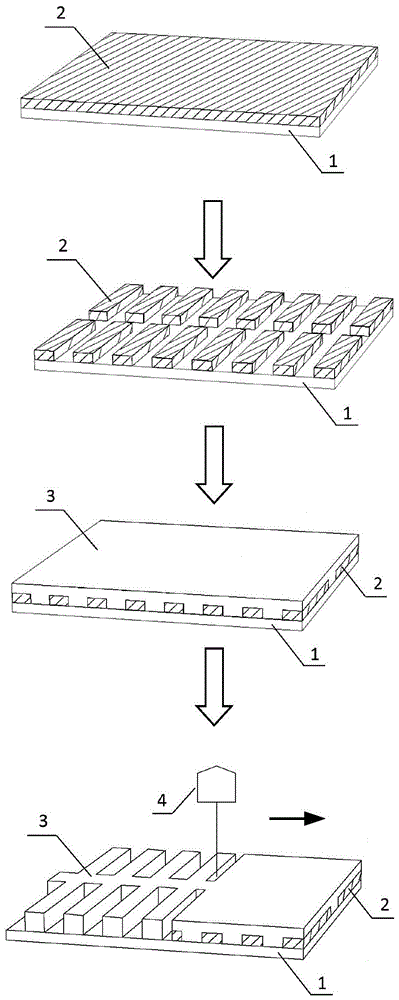
[0024] Such as figure 1 Shown, the preparation method of patterned organic thin film comprises the following steps:

[0025] Step 1. Prepare a patterned substrate film layer 2 with a thickness of 5-100 nm on the upper surface of the substrate 1. The specific preparation method is not particularly limited, and a method well known to those skilled in the art can be used, such as inkjet printing or silk Screen printing can directly prepare a patterned substrate film layer 2 with a thickness of 5-100 nm on the upper surface of the substrate 1; 100nm of the substrate film layer, and then prepare the patterned substrate film layer 2 by nanoimprinting, mechanical lift-off or laser etching.

[0026] The material of the substrate 1 is not particularly limited, and a PET flexible substrate, an ITO conductive substrate or a glass substrate is generally used.

[0027] The material of the patterned substrate film layer 2 has absorption capacity in the infrared band, and is generally a PE...

Embodiment 1

[0034] Methods for patterning organic thin films:

[0035]Step 1. A PEDOT:PSS film with a thickness of 5 nm is prepared by spin coating on the upper surface of the glass substrate. The spin coating solution is commercially available PEDOT:PSS, and the model is Al4083;

[0036] Step 2: Utilize the laser etching method to pattern the PEDOT:PSS film. The patterned substrate film layer 2 is composed of a plurality of identical cuboids, and the plurality of cuboids are symmetrically distributed in pairs along an axis. The length of all cuboids is The sides are all parallel, and the sides of the cuboid on the same side of the axis are on the same plane. After patterning, the surface of part of the glass substrate is exposed, and a patterned PEDOT:PSS film is obtained;

[0037] Step 3. Spin-coat 50 nm thick P3HT:PC with a mass ratio of 1:1 on the upper surface of the patterned PEDOT:PSS film and the exposed glass substrate 61 BM blends to give P3HT:PC 61 BM blend layer;

[0038] S...

Embodiment 2

[0040] Methods for patterning organic thin films:

[0041] Step 1. Prepare a patterned PEDOT:PSS film on the upper surface of the PET substrate by inkjet printing or screen printing. The ink is a PEDOT:PSS original solution with a volume ratio of 18:9:73 and deionized water. , a mixture of isopropanol;

[0042] Step 2. Spin-coat 100 nm thick PBDT-TFQ:PC with a mass ratio of 1:1 on the upper surface of the patterned PEDOT:PSS film and the exposed PET substrate 71 BM blends to give PBDT-TFQ:PC 71 BM blend layer;

[0043] Step 3. Use an infrared laser source with a wavelength range of 1000nm to scan PBDT-TFQ:PC point by point 71 BM blend layer with a laser energy density of 2J / cm 2 , the patterned PEDOT:PSS film absorbs infrared light and generates heat, and the PBDT-TFQ:PC on it 71 BM blend layer burned off, PBDT-TFQ:PC on bare PET substrate 71 The BM blend was retained, resulting in an organic film with a pattern complementary to that of the patterned PEDOT:PSS film.


PUM

PropertyMeasurementUnit
thicknessaaaaaaaaaa
thicknessaaaaaaaaaa
wavelengthaaaaaaaaaa

Abstract

The present invention disclosed a method of preparing a pattern organic film, which is the field of organic film pattern technology.When solving the method of organic film pattern in existing technologies, when laser etching on the processing layer, it is easy to cause technical problems to cause heat damage to non -processing layers adjacent to the processing layer.This method first prepares patterns on the surface of the base to prepare a thin -len film layer, and then prepare a single layer or composite organic film layer on the surface of the pattern thinner film layer and the naked base.Single -layer or composite organic thin film layer, using organic thin film materials and substrate thin film materials to absorb infrared light to absorb the heat of the substrate thin film layer to absorb calories, burn the single layer or composite organic thin film layer on itThe single layer or composite organic film layer on the surface of the exposed base is retained to obtain a pattern organic film.This method does not require the pulse width of the laser, the processing quality is easy to ensure, and the cost is low.

Description

technical field [0001] The invention relates to the technical field of organic film patterning, in particular to a method for preparing a patterned organic film. Background technique [0002] Patterned organic thin films are widely used in organic electronics such as organic solar cells, organic transistors, and organic light-emitting diodes. Existing methods for patterning organic thin films mainly include inkjet printing, screen printing, nanoimprinting, and laser etching. Among them, the laser etching method is often used to prepare high-performance devices due to its advantages of high precision, high speed and strong flexibility. [0003] In the preparation of high-precision patterned organic thin films by laser etching, especially in the patterned processing of multi-layer thin films, when the layer to be processed (etched layer) is laser etched, it is easy to damage the non-layer adjacent to the layer to be processed. The processing layer (non-etching layer) causes ...

Claims


Application Information

Patent Timeline
Patent Type & Authority Patents(China)
IPC IPC(8): H01L51/56H01L51/00H10K99/00
CPCH10K71/20H10K71/00
Inventor 杨小牛叶峰赵晓礼张通吴凡吕红英
Owner CHANGCHUN INST OF APPLIED CHEMISTRY - CHINESE ACAD OF SCI
Learn More