Preparation method of intermetallic compound film

A technology of intermetallic compounds and thin films, which is applied in the field of preparation of intermetallic compound thin films, can solve the problems of slow growth rate, high energy consumption and high cost of thin films, and achieve the effects of accelerated growth rate, fast growth rate and improved mechanical properties

Active Publication Date: 2015-06-03
DALIAN UNIV OF TECH
View PDF3 Cites 0 Cited by
  • Summary
  • Abstract
  • Description
  • Claims
  • Application Information

AI Technical Summary

Problems solved by technology

However, the above method has the following disadvantages: it needs to be prepared under high temperature and vacuum environment, and has a strong dependence on equipment; it consumes a lot of energy and costs high; the film growth rate is slow

Method used


Image

  • Preparation method of intermetallic compound film
  • Preparation method of intermetallic compound film
  • Preparation method of intermetallic compound film

Examples


Embodiment 1

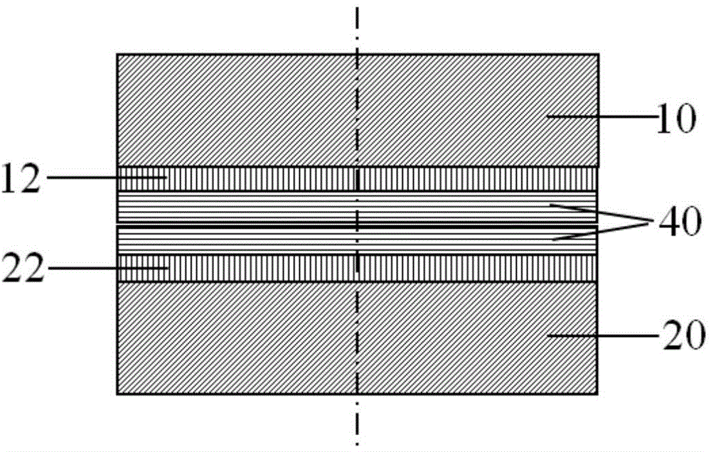
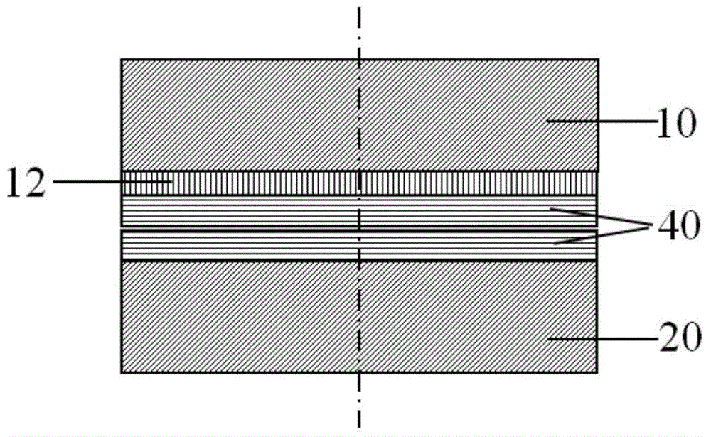
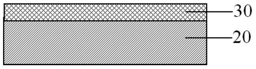
[0044] Such as figure 1 and image 3Shown, the preparation method of intermetallic compound thin film of the present invention can be realized by following specific processing steps:

[0045] Step 1: Provide a polycrystalline Cu first metal substrate, sputter a 0.25 μm thick Sn first solder metal layer on the polycrystalline Cu first metal substrate; provide a polycrystalline Cu second metal substrate, and sputter on the polycrystalline Cu first metal substrate. Sputtering a 0.25 μm thick Sn second solder metal layer on the crystal Cu second metal substrate;

[0046] Step 2: coating flux on the surfaces of the first Sn solder metal layer and the Sn second solder metal layer;

[0047] Step 3: Aligning the first Sn solder metal layer and the Sn second solder metal layer, and placing them in contact to form an assembly;

[0048] Step 4: Heat the assembly formed in Step 3 to 250° C. for brazing reflow, and make the temperature of the polycrystalline Cu first metal substrate low...

Embodiment 2

[0052] Such as figure 1 and image 3 Shown, the preparation method of intermetallic compound thin film of the present invention can be realized by following specific processing steps:

[0053] Step 1: providing a polycrystalline Cu first metal substrate, electroplating a 10 μm thick Sn-Cu first solder metal layer on the polycrystalline Cu first metal substrate; providing a polycrystalline Cu second metal substrate, on the polycrystalline Cu first metal substrate, Electroplating a 10 μm thick Sn-Cu second solder metal layer on the Cu second metal substrate;

[0054] Step 2: Coating flux on the surfaces of the first Sn-Cu solder metal layer and the Sn-Cu second solder metal layer;

[0055] Step 3: aligning the Sn-Cu first solder metal layer and the Sn-Cu second solder metal layer, and placing them in contact to form an assembly;

[0056] Step 4: Heat the assembly formed in Step 3 to 250° C. for brazing reflow, and make the temperature of the polycrystalline Cu first metal sub...

Embodiment 3

[0060] Such as figure 1 and image 3 Shown, the preparation method of intermetallic compound thin film of the present invention can be realized by following specific processing steps:

[0061] Step 1: Provide a polycrystalline Cu first metal substrate, electroplate a 30 μm thick Sn first solder metal layer on the polycrystalline Cu first metal substrate; provide a polycrystalline Cu second metal substrate, and Electroplating a second solder metal layer of Sn with a thickness of 30 μm on the second metal base;

[0062] Step 2: coating flux on the surfaces of the first Sn solder metal layer and the Sn second solder metal layer;

[0063] Step 3: Aligning the first Sn solder metal layer and the Sn second solder metal layer, and placing them in contact to form an assembly;

[0064] Step 4: Heat the assembly formed in Step 3 to 250° C. for brazing reflow, and make the temperature of the polycrystalline Cu first metal substrate lower than the temperature of the polycrystalline Cu ...


PUM

PropertyMeasurementUnit
thicknessaaaaaaaaaa

Abstract

The invention discloses a preparation method of an intermetallic compound film. The preparation method comprises the following steps: preparing a first brazing filler material metal layer on a first metal base, and preparing a second brazing filler material metal layer on a second metal base, and aligning, contacting and placing the first brazing filler material metal layer and the second brazing filler material metal layer which are coated with welding fluxes to form a composite solid; or aligning the first brazing filler material metal layer and the second brazing filler material metal layer, contacting and placing to form the composite solid; heating the composite solid to required temperature, refluxing the brazing so as to form temperature gradient between the first metal base and the second base until the brazing filler material meta layers are molten to play the brazing reaction, completely transforming the brazing filler material metal layers into the intermetallic compound, removing residual second metal base to obtain the intermetallic compound film. The temperature gradient is formed when the brazing is refluxed, the forming rate of the intermetallic compound is accelerated, and the formed intermetallic compound can be single crystal or is provided with single orientation; the low-temperature preparation of the intermetallic compound film is realized, the film is compact, the surface is smooth, and the film-forming quality is good.

Description

technical field [0001] The invention belongs to the field of functional materials and relates to a preparation method of an intermetallic compound thin film. Background technique [0002] Intermetallic compounds have diverse bonding types (metallic bonds and covalent bonds), special crystal structures, electronic structures, and energy band structures, and thus have many special physical, chemical and mechanical properties. For example, unique electrical properties, magnetic properties, optical properties, acoustic properties, electron emission properties, catalytic properties, oxidation resistance and corrosion resistance. Intermetallic compounds can not only be used as high-temperature structural materials, but also have a very wide range of applications in the field of functional materials, such as semiconductor materials, magnetic materials, memory alloys, hydrogen storage materials, high-brightness electron source materials, and catalysts. However, due to the brittlene...

Claims


Application Information

Patent Timeline
Patent Type & Authority Applications(China)
IPC IPC(8): C30B11/00C30B29/52
Inventor 黄明亮赵宁杨帆张志杰邓建峰赵杰
Owner DALIAN UNIV OF TECH
Why Eureka
Try Eureka