Self-aligning double patterning formation method

A dual-patterning and self-aligning technology, which is applied in the photoengraving process, optics, instruments and other directions of the patterned surface, can solve the problems of poor semiconductor structure and unstable performance, and achieve stable and good surface morphology. Improve and enhance the effect of strength

Active Publication Date: 2015-06-10
SEMICON MFG INT (SHANGHAI) CORP
View PDF5 Cites 19 Cited by
  • Summary
  • Abstract
  • Description
  • Claims
  • Application Information

AI Technical Summary

Problems solved by technology

[0009] However, the semiconductor structure formed by mask etching formed by the existing self-aligned double patterning process has poor morphology and unstable performance

Method used


Image

  • Self-aligning double patterning formation method
  • Self-aligning double patterning formation method
  • Self-aligning double patterning formation method

Examples


Embodiment Construction

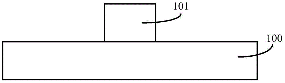
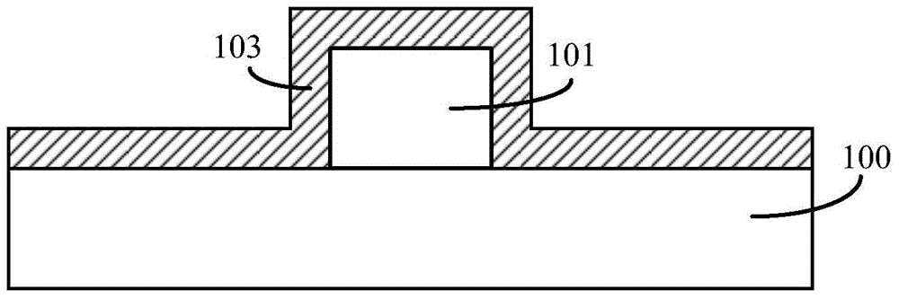
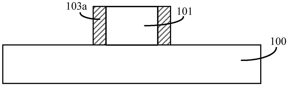
[0026] As mentioned in the background art, the semiconductor structure formed by mask etching formed by the existing self-aligned double patterning process has poor morphology and unstable performance.

[0027] After research, please continue to refer to Figures 1 to 4 , when etching the layer 100 to be etched with the mask sidewall 103a, the shape of the mask sidewall 103a will cause damage, and the semiconductor structure to be etched by the layer 100 to be etched will have poor morphology and inaccurate dimensions. . Wherein, the formation process of the sacrificial layer 101 is a photolithography process, including: forming a sacrificial film on the surface of the layer to be etched 100, forming a bottom anti-reflection layer on the surface of the sacrificial film, forming a photoresist layer on the surface of the bottom anti-reflection layer, The photoresist layer is exposed for patterning; using the photoresist layer as a mask, the anti-reflection layer and the sacrifi...


PUM


Abstract

A self-aligning double patterning formation method includes providing a to-be-etched layer, wherein the surface of the to-be-etched layer is provided with a plurality of discrete sacrificial layers; forming mask layers on the surface of the to-be-etched layer and the sidewall and top surfaces of the sacrificial layers; etching back the mask layers until the mask layers expose out of the surface of the to-be-etched layer and the top surfaces of the sacrificial layers, and forming mask spacers on the sidewall surfaces of the sacrificial layers; removing the sacrificial layers after the mask spacers are formed; after the sacrificial layers are removed, subjecting the mask spacers to strengthening treatment to enable the mask spacers to be densified. The masks formed by self-aligning double patterning process are good in shape.

Description

technical field [0001] The invention relates to the technical field of semiconductor manufacturing, in particular to a method for forming a self-aligned double pattern. Background technique [0002] With the continuous progress of semiconductor technology, the process nodes of semiconductor devices are continuously reduced. However, due to the limitation of the precision of the existing photolithography process, the mask pattern formed by the existing photolithography process is difficult to meet the demand for continuous reduction of the feature size of semiconductor devices, which hinders the development of semiconductor technology. [0003] In order to further reduce the size of the semiconductor device on the basis of the existing photolithography process, a double patterning process is proposed in the prior art. Among them, the self-aligned double patterning (Self-Aligned Double Patterning, SADP) process is widely used because of its simplicity. Figure 1 to Figure 4 I...

Claims


Application Information

Patent Timeline
Patent Type & Authority Applications(China)
IPC IPC(8): H01L21/311
CPCG03F7/70466H01L21/311H01L21/31144
Inventor 刘佳磊
Owner SEMICON MFG INT (SHANGHAI) CORP
Why Eureka
Try Eureka