Method for forming shallow trench

A shallow trench and amorphous carbon technology, which is applied in the manufacture of electrical components, semiconductor/solid-state devices, and circuits, can solve the problems of large differences in the depth of shallow trenches and lower yields, so as to alleviate the difference in etching amount and ensure The effect of yield

Active Publication Date: 2015-06-10
SEMICON MFG INT (SHANGHAI) CORP
View PDF5 Cites 0 Cited by
  • Summary
  • Abstract
  • Description
  • Claims
  • Application Information

AI Technical Summary

Problems solved by technology

[0008] However, the depth of the shallow grooves formed by the prior art vari

Method used


Image

  • Method for forming shallow trench
  • Method for forming shallow trench
  • Method for forming shallow trench

Examples


Example Embodiment

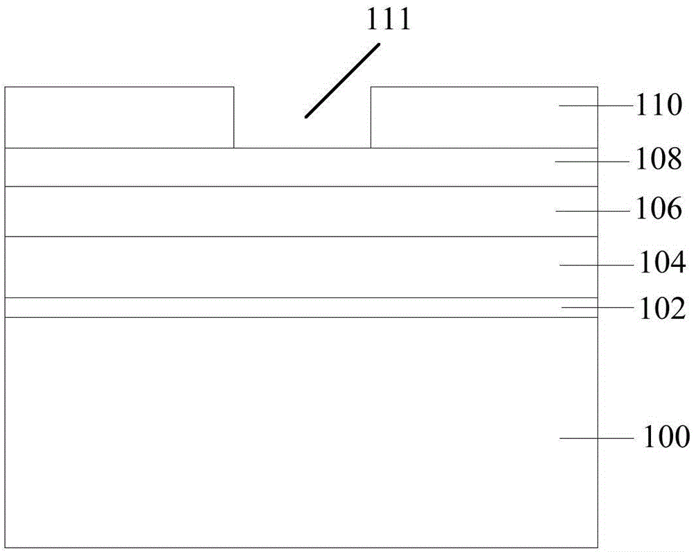
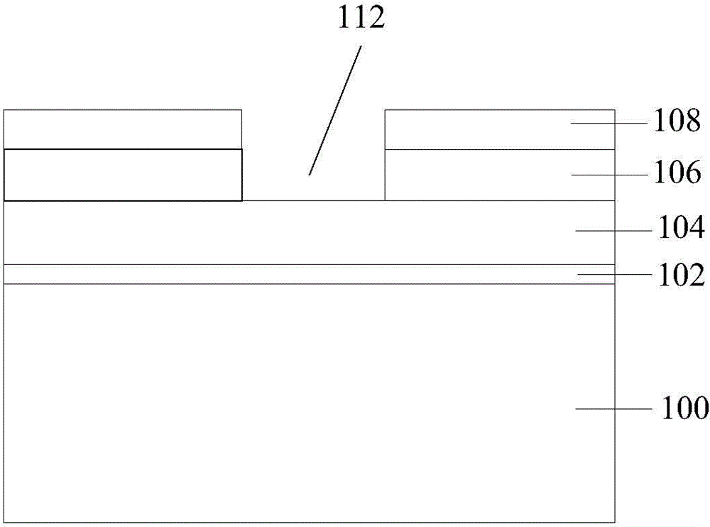
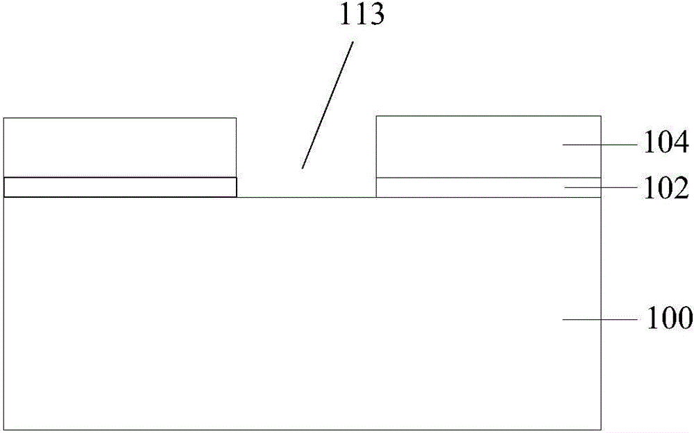
[0033] In the existing process of forming shallow trench isolation to separate the active regions, due to the slight asymmetry of plasma distribution in the reaction chamber, or the slight difference in etching rate, it will cause the film in different positions of the wafer after the same process step. The amount to be etched will vary, and if a multi-step etching process is required to form a shallow trench, the difference will be accumulated, so that the depth of the final shallow trench will vary greatly at different positions, which will reduce the yield.

[0034] To solve this problem, in the process of forming shallow trenches, the present invention adjusts the horizontal angle of the wafer before each step of etching, so that the final adjusted angle is consistent with the maximum asymmetry, so as to alleviate the unevenness of the etching amount. Make the depth of the finally formed shallow trench consistent at different positions, ensuring the yield of semiconductor devi...


PUM


Abstract

The invention relates to a method for forming a shallow trench, comprising the following steps: providing a semiconductor substrate, wherein N film layers are sequentially formed on the surface of the semiconductor substrate from bottom to top, and N is a positive integer; and sequentially etching the film layers step by step from top to bottom until a shallow trench is formed in the semiconductor substrate, wherein a wafer is horizontally rotated by a predetermined angle before each step of etching. According to the method of the invention, the wafer is constantly rotated by a certain angle before next step of etching to alleviate the difference between different positions in the amount of etching, so that the ultimately formed shallow trench has uniform depth in different positions, and the yield rate of semiconductor devices is ensured.

Description

technical field [0001] The invention relates to the technical field of semiconductors, in particular to a method for forming shallow trenches. Background technique [0002] As the size of integrated circuits decreases, the devices that make up the circuits must be placed more densely to fit the limited space available on the chip. Since current research is devoted to increasing the density of active devices per unit area of ​​a semiconductor substrate, effective insulating isolation between circuits becomes more important. [0003] Shallow trench isolation (STI) technology has a number of process and electrical isolation advantages, including reducing the area occupied by the wafer surface while increasing the integration of devices, maintaining surface flatness and reducing channel width erosion. Therefore, at present, active region isolation layers of components such as MOS circuits are mostly manufactured by shallow trench isolation technology. The specific process step...

Claims


Application Information

Patent Timeline
IPC IPC(8): H01L21/762
CPCH01L21/76224
Inventor 张海洋王冬江
Owner SEMICON MFG INT (SHANGHAI) CORP
Why Eureka
Try Eureka