PCB of power circuit for automobile instrument and design method of PCB
A technology for PCB boards and automotive instruments, applied in printed circuits, printed circuits, circuit thermal devices, etc., can solve problems such as low work efficiency, unfavorable production line production, unstable voltage output, etc., to improve work efficiency, prolong service life, The effect of increasing the heat dissipation rate
- Summary
- Abstract
- Description
- Claims
- Application Information
AI Technical Summary
Problems solved by technology
Method used
Image
Examples
specific Embodiment approach 1
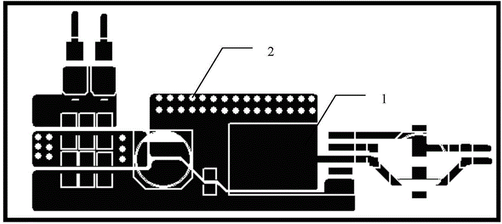
[0023] Specific implementation mode one: refer to figure 2 Describe this embodiment in detail, the PCB board of the power supply circuit for automobile instrument described in this embodiment, the pad of each heating element is covered with a large-area top layer copper clad layer 1, and the area of the top layer copper clad layer 1 10 times larger than the pad area of the heating element.
[0024] In the PCB board of the power supply circuit for automobile instrument described in this embodiment, the pads of each heating element are all covered with a large-area top layer copper clad layer 1. Since copper has good thermal conductivity, the number of pads connected to the heating element is increased. The area of the copper layer can quickly dissipate the heat on the component to the connected copper layer, so that the heat will not accumulate on the component, effectively prevent the damage of the heating component due to the long working time and temperature rise, and...
specific Embodiment approach 2
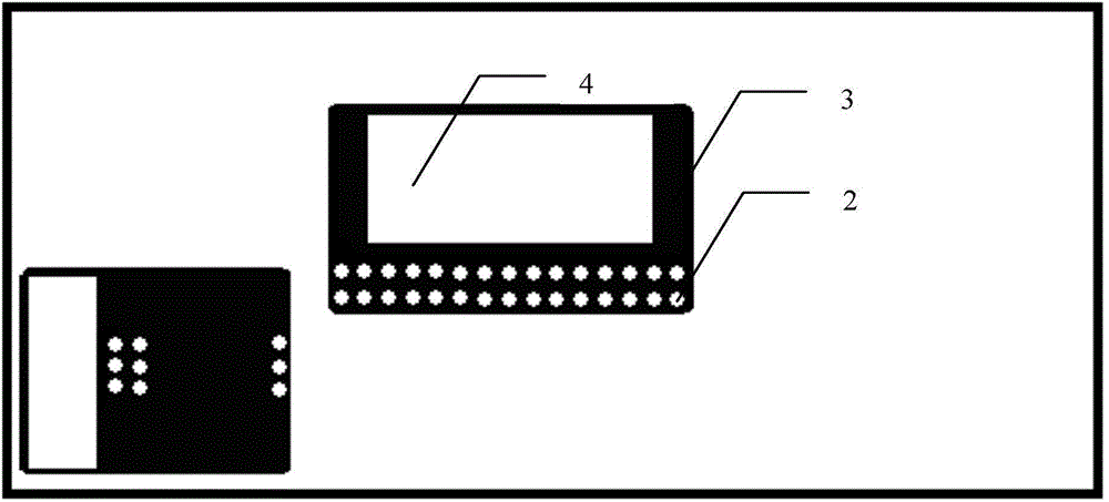
[0025] Specific implementation mode two: see image 3 This embodiment will be described. This embodiment is a further description of the PCB board of the power supply circuit for automobile instrument described in Embodiment 1. In this embodiment, a plurality of via holes 2 are opened on the top copper clad layer 1 on the PCB, and there The bottom layer of the PCB board corresponding to each via hole 2 is covered with a bottom copper clad layer 3 .
[0026] In this embodiment, a copper clad layer 3 for heat dissipation is added to the bottom layer of the PCB, so that the heat is distributed on the top and bottom layers of the PCB, and the heat dissipation can be effectively accelerated.
specific Embodiment approach 3
[0027] Specific implementation mode three: refer to image 3 This embodiment is described in detail. This embodiment is to further illustrate the PCB board of the power supply circuit for automobile instrument described in the second specific embodiment. In this embodiment, the bottom copper clad layer 3 of the PCB bottom layer and the corresponding top layer copper The area of the layer 1 is close, and the bottom cladding copper layer 3 partially overlaps with the corresponding top copper cladding layer 1 .
[0028] In this embodiment, the areas of the bottom copper clad layer 3 and the top copper clad layer 1 are similar, so that the heat dissipation of the top layer and the bottom layer of the PCB board is similar. The bottom cladding copper layer 3 partially overlaps with the corresponding top copper clad layer 1 , that is, it only overlaps the part of the via hole 2 , and the via hole 2 transfers the heat of the top copper clad layer to the bottom copper clad layer 3 . ...
PUM
 Abstract
Description
Claims
Application Information


