

Polycrystalline silicon ingot, manufacturing method thereof, and crucible
A technology for polycrystalline silicon ingots and crucibles, which is applied in the field of crucibles, polycrystalline silicon ingots and their manufacturing methods, can solve the problems such as the difficulty in improving the conversion efficiency of solar cells, and achieve the effects of consistent crystal grain orientation, uniform distribution, and improved conversion efficiency
- Summary
- Abstract
- Description
- Claims
- Application Information
AI Technical Summary
Problems solved by technology
Method used
Image

Examples
Embodiment Construction
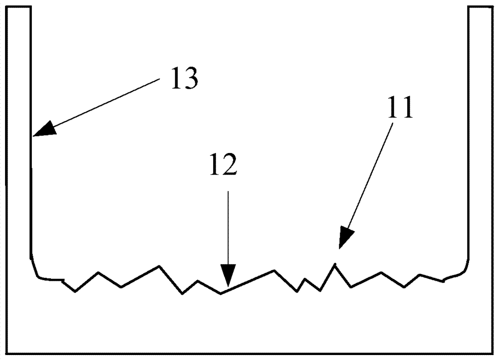
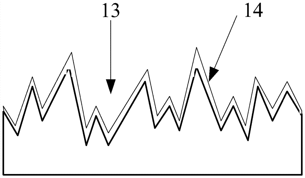
[0031] As mentioned in the background technology section, the quality of polycrystalline silicon ingots obtained by using the ingot casting process in the prior art is poor, and the conversion efficiency of solar cells made by using polycrystalline silicon ingots in the prior art is low. The inventors have found that this problem occurs The reason is that in the polycrystalline silicon ingot in the prior art, during the crystal growth process, the crystal nucleates and grows randomly, resulting in a large difference in the size of the crystal grains in the finally formed silicon ingot, and there will be some inclusions between the large crystal grains. Small grains, or defects such as subgrain boundaries are distributed inside large grains, and the size of small grains is too small, resulting in many grain boundaries and dislocations inside the silicon ingot, and these defects such as subgrains and dislocations are very easy to It becomes the recombination center of photogenera...
PUM
 Abstract
Description
Claims
Application Information