Array substrate, manufacturing method thereof and display device

A technology for array substrates and display areas, which is applied in semiconductor/solid-state device manufacturing, semiconductor devices, electrical components, etc., and can solve problems such as performance degradation and damage of semiconductor layer metal wiring

Active Publication Date: 2015-06-17
BOE TECH GRP CO LTD
View PDF3 Cites 3 Cited by
  • Summary
  • Abstract
  • Description
  • Claims
  • Application Information

AI Technical Summary

Problems solved by technology

Since the insulating glass substrate cannot eliminate the accumulation of static electricity by itself, there will be an obvious potential difference between the conductive part on the array substrate. Once

Method used


Image

  • Array substrate, manufacturing method thereof and display device
  • Array substrate, manufacturing method thereof and display device
  • Array substrate, manufacturing method thereof and display device

Examples


preparation example Construction

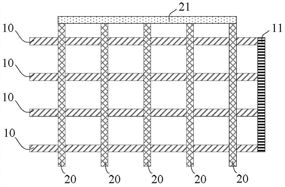
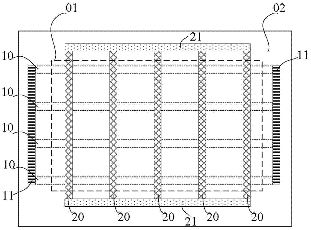
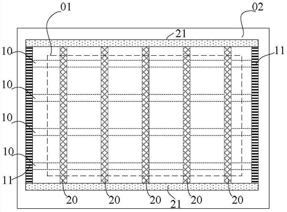
[0031] An embodiment of the present invention provides a method for preparing an array substrate, including forming a thin film transistor and a signal line, and further comprising forming a signal line connection line, wherein the signal line connection line at least electrically connects the same type of signal line; Before the last film layer of the array substrate manufacturing process is completed, the method further includes: etching a via hole on the connecting line of the signal line or at a position where the signal line is close to the connecting line of the signal line, the The vias are used to disconnect the electrical connection between the signal lines.

[0032] It should be noted that, first, the type of the signal line is not limited, as long as it is formed on the array substrate and may generate electrostatic discharge with other conductors. For example: the signal line may be a gate line, or a data line, or a common electrode line and the like.

[0033] Whe...


PUM


Abstract

The embodiment of the invention provides an array substrate, a manufacturing method thereof and a display device, and relates to the technical field of display. The electrostatic discharge of the TFT array substrate in the manufacturing process can be effectively reduced, and the product yield is improved. The method includes the step of forming a thin film transistor and signal lines and further includes the step of forming a signal line communicating wire, wherein the signal line communicating wire at least makes the signal lines of the same type electrically connected. Before the last film layer is manufactured in the array substrate manufacturing process, the method further includes the step of etching via holes in the signal line communicating wire or the positions, close to the signal line communicating wires, of the signal lines, wherein the via holes are used for eliminating the electrical connection of the signal lines. The method is used for manufacturing the array substrate and the display device.

Description

technical field [0001] The present invention relates to the field of display technology, in particular to an array substrate, a preparation method thereof, and a display device. Background technique [0002] In the production process of Thin-Film Transistor (TFT) array substrates, static electricity accumulation often occurs, and due to the display requirements, insulating glass substrates are used, resulting in the static electricity accumulation during the production process. Therefore, it is easy to cause the problem of Electro-Static Discharge (ESD for short), which will cause the performance of the array substrate to degrade or even be destroyed, thereby reducing the product yield. [0003] Specifically, in the manufacturing process of thin film transistors, some process environments will generate static electricity accumulation, such as: chemical vapor deposition (Chemical Vapor phase Deposition, CVD for short), sputtering (sputtering) or dry etching and other plasma-r...

Claims


Application Information

Patent Timeline
IPC IPC(8): H01L27/12H01L21/77
CPCH01L27/0288H01L27/124H01L21/77H01L27/12H01L21/76805H01L21/76892H01L27/1244H01L27/1248H01L27/1259
Inventor 李全虎李永谦王龙彦
Owner BOE TECH GRP CO LTD
Why Eureka
Try Eureka