Thin film transistor and production method of thin film transistor, array substrate and display equipment

A technology of thin film transistor and manufacturing method, which is applied in transistor, semiconductor/solid-state device manufacturing, semiconductor device and other directions, can solve the problems of poor display quality, uneven gate line resistance, and gate line bulging.

Inactive Publication Date: 2015-06-17
HEFEI XINSHENG OPTOELECTRONICS TECH CO LTD +1
View PDF7 Cites 5 Cited by
  • Summary
  • Abstract
  • Description
  • Claims
  • Application Information

AI Technical Summary

Problems solved by technology

[0006] In summary, in the process of producing thin film transistors in the prior art, the problem of gate line bulging is prone to occur, which makes the resistance of the gate line uneven, which in turn leads to uneven display and poor display quality of the display.

Method used


Image

  • Thin film transistor and production method of thin film transistor, array substrate and display equipment
  • Thin film transistor and production method of thin film transistor, array substrate and display equipment
  • Thin film transistor and production method of thin film transistor, array substrate and display equipment

Examples


Embodiment 1

[0049] see image 3 , a method for fabricating a thin film transistor provided in an embodiment of the present invention includes:

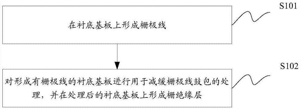
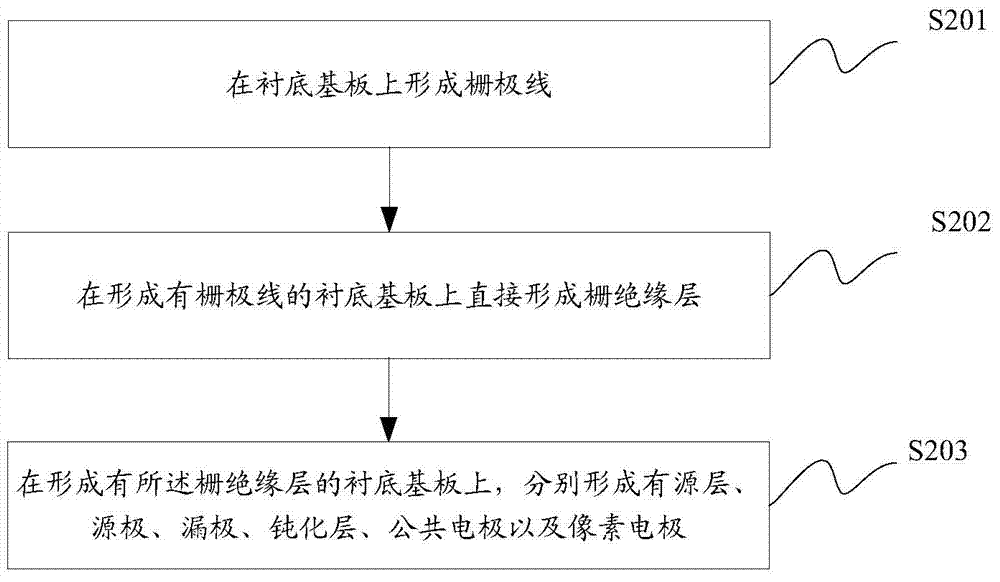
[0050] S201, forming a gate line on the base substrate;

[0051] S202, directly forming a gate insulating layer on the base substrate on which the gate lines are formed;

[0052] In this embodiment, the gate insulating layer is directly formed on the base substrate on which the gate line is formed, that is, the N2 plasma treatment step is omitted. Since the plasma treatment is to obtain plasma by heating for bombardment treatment, omitting this step will greatly reduce the The temperature at which the gate lines are heated reduces the temperature at which the gate lines are heated and prevents the grid lines from bulging.

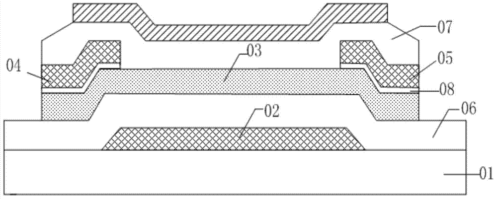
[0053] S203 , respectively forming an active layer, a source electrode, a drain electrode, a passivation layer, a common electrode, and a pixel electrode on the base substrate on which the gate insulating layer is formed.

Embodiment 2

[0055] see Figure 4 , a method for fabricating a thin film transistor provided in an embodiment of the present invention includes:

[0056] S301, forming a gate line on the base substrate;

[0057] S302. Perform plasma treatment on the gate lines with a preset plasma treatment power, and form a gate insulating layer on the base substrate on which the gate lines are formed after the plasma treatment, wherein the preset plasma treatment The power is less than 8 kW.

[0058] In this embodiment, the power of the plasma treatment is reduced. Since the plasma treatment is bombarded by heated plasma, reducing the power of the plasma treatment also reduces the temperature of the plasma treatment, thereby reducing the heating temperature of the grid line and avoiding the grid line. Extreme line drum kit.

[0059] S303 , respectively forming an active layer, a source electrode, a drain electrode, a passivation layer, a common electrode, and a pixel electrode on the base substrate on...

Embodiment 3

[0061] see Figure 5 , a method for fabricating a thin film transistor provided in an embodiment of the present invention includes:

[0062] S401, forming a gate line on the base substrate;

[0063] S402. According to the preset preheating time, perform preheating treatment on the base substrate formed with the gate lines, and form a gate insulating layer on the preheated base substrate formed with the gate lines, wherein the The preset warm-up time mentioned above is less than 60 seconds;

[0064] In this embodiment, by reducing the preheating time, the heating time of the gate lines is shortened, thereby reducing the temperature at which the gate lines are heated, and avoiding the swelling of the gate lines.

[0065] Through specific experiments, it can be known that when the preheating time is within the range of 10 seconds and 20 seconds, the swelling problem of the gate lines will be alleviated to the greatest extent, and the oxidation degree of the gate lines will be s...


PUM


Abstract

The invention discloses a thin film transistor and a production method of the thin film transistor, an array substrate and display equipment, aiming at slowing down and even avoiding the problem of gate line bulging in a production process for the thin film transistor, so that the resistance of a gate line is uniform, and then the display effect of a display is uniform, and the display quality of the display is improved. The method comprises the following steps: forming the gate line on a substrate; carrying out processing of slowing down the gate line bulging on the substrate on which the gate line is formed, and forming a gate insulation layer on the processed substrate.

Description

technical field [0001] The invention relates to the technical field of displays, in particular to a thin film transistor, a manufacturing method thereof, an array substrate, and a display device. Background technique [0002] In the production of display devices, thin-film transistors (Thin-film Transistor, TFT) play a very important role. The on-state of the thin-film transistor is used to quickly charge the pixel capacitance of the display device, and the off-state of the thin-film transistor is used to maintain the pixel. Capacitor voltage, which achieves unity of fast response and good storage. Thin film transistors are widely used as nonlinear switching elements in large-area liquid crystal displays and contact image sensors due to their very high ratio of on-state current (Ion) to off-state current (Ioff) and steep transfer characteristics. . [0003] The specific structure of the current conventional bottom-gate anti-stacked amorphous silicon thin film transistor is...

Claims


Application Information

Patent Timeline
Patent Type & Authority Applications(China)
IPC IPC(8): H01L29/786H01L21/336H01L27/12
CPCH01L27/124H01L29/6675H01L29/78672H01L21/0217H01L21/02315H01L21/321H01L29/42384H01L29/66765H01L27/1255H01L29/4908H01L29/66742H01L27/1222
Inventor 邹志翔操彬彬黄寅虎
Owner HEFEI XINSHENG OPTOELECTRONICS TECH CO LTD
Why Eureka
Try Eureka