
A Method for Realizing Nanoscale Overlay Accuracy by Microscopy

An overlay precision and microscope technology, which is applied in the direction of microlithography exposure equipment, photoplate making process exposure device, etc., can solve the problems that affect the final product yield, low accuracy of human eye recognition, large error, etc., and achieve the reduction of online overlay. The effect of accuracy failure rate, reduction of rework frequency, and improvement of detection accuracy

Active Publication Date: 2017-02-22
SHANGHAI HUALI MICROELECTRONICS CORP
View PDF7 Cites 0 Cited by
  • Summary
  • Abstract
  • Description
  • Claims
  • Application Information

AI Technical Summary

Problems solved by technology

[0006] The present invention aims at correcting the offset between the pattern of the current layer and the pattern of the previous layer in the prior art, often due to the low recognition accuracy of human eyes and large errors, which will lead to artificial deviation, and will also affect the final result due to insufficient accuracy. Defects such as product yield provide a method to achieve nanoscale overlay accuracy through microscopy

Method used


Image

  • A Method for Realizing Nanoscale Overlay Accuracy by Microscopy
  • A Method for Realizing Nanoscale Overlay Accuracy by Microscopy
  • A Method for Realizing Nanoscale Overlay Accuracy by Microscopy

Examples


Embodiment Construction

[0023] In order to illustrate the technical content, structural features, achieved goals and effects of the present invention in detail, the following will be described in detail in conjunction with the embodiments and accompanying drawings.

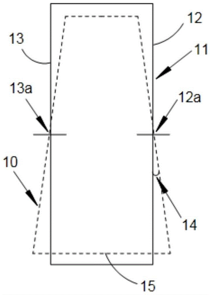
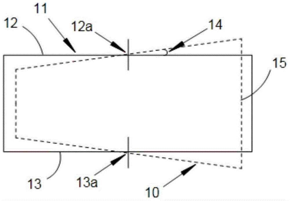
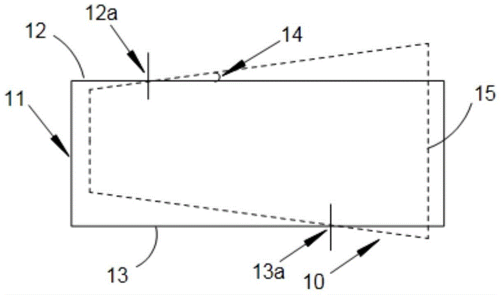
[0024] see figure 1 , figure 1 Shown is a schematic diagram of the principle of the method for realizing nanoscale overlay precision through microscopy in the present invention. The method for realizing nanoscale overlay precision by microscopy includes:

[0025] Execute step S1: provide a mask plate (not shown) with the current layer pattern 10, when the overlay accuracy of the current layer pattern 10 of the mask plate and the defined previous layer pattern 11 is zero, the current layer pattern 10 and the front layer pattern 11 have a first intersection point 12a and a second intersection point 13a on the first boundary 12 and the second boundary 13 that are set opposite to each other in the first direction, and the first intersectio...


PUM

PropertyMeasurementUnit
wavelengthaaaaaaaaaa

Abstract

The invention discloses a method for achieving nanoscale alignment precision by employing a microscopic method. The method comprises the steps as follows: when the alignment precision of a current layer of pattern of a mask plate and a previous layer of pattern of the mask plate is zero, the offset of a first intersection point and a second intersection point is zero; when the included angle between the current layer of pattern and the previous layer of pattern is theta, the computation formula of theta is shown in the specification; L1 is the distance from the bottom angle of the current layer of pattern to a first boundary of the previous layer of pattern; H1 is the distance from the first intersection point to the bottom edge of the current layer of pattern; the offset in a second direction is L2-L1; the offset of the first intersection point and the second intersection point in a first direction is L3 by adopting a microscopic method; the computation formula is shown in the specification; and the offset of the current layer of pattern and the previous layer of pattern in the second direction is shown in the specification. The method is a process of meeting the requirement of high alignment precision; the detection accuracy is improved; the reject ratio of on-line alignment precision of a silicon slice is reduced; the rework frequency is reduced; and the device performance of a product is finally improved and the yield of the product is finally increased.

Description

technical field [0001] The invention relates to the technical field of semiconductor manufacturing, in particular to a method for realizing nanoscale overlay precision through microscopy. Background technique [0002] At present, in the semiconductor manufacturing process, the correction of the positional deviation of the previous layer pattern and the current layer pattern is usually realized by aligning the vernier. However, the low accuracy and large error of human eye recognition will not only cause human error due to individual differences in testing, but also affect the final product yield due to insufficient accuracy. [0003] For example, when the alignment result is shifted to the right by one grid, the actual error judgment is performed according to the offset between the designed cursor on the previous layer and the cursor on the current layer. In the industry, the existing technology can only realize the overlay deviation detection of 0.4 μm, which cannot satisf...

Claims


Application Information

Patent Timeline
Patent Type & Authority Patents(China)
IPC IPC(8): G03F7/20
Inventor 蔡亮吴鹏陈力钧
Owner SHANGHAI HUALI MICROELECTRONICS CORP
Learn More