Double-bit flash memory, and programming, erasing and reading method thereof

A flash memory and control gate technology, which is applied in the semiconductor field to achieve the effects of increasing storage density, reducing size and increasing storage capacity

Inactive Publication Date: 2015-06-24
SHANGHAI HUALI MICROELECTRONICS CORP
View PDF5 Cites 4 Cited by
  • Summary
  • Abstract
  • Description
  • Claims
  • Application Information

AI Technical Summary

Problems solved by technology

The single-gate floating gate flash memory structure causes each storage unit to only distinguish between two different states, that is, "0" and "1", so that each storage unit has only 2bit (bit, bit) storage capacity

Method used


Image

  • Double-bit flash memory, and programming, erasing and reading method thereof
  • Double-bit flash memory, and programming, erasing and reading method thereof

Examples


Embodiment Construction

[0028] The specific embodiment of the present invention will be further described in detail below in conjunction with the accompanying drawings.

[0029] It should be noted that, in the following specific embodiments, when describing the embodiments of the present invention in detail, in order to clearly show the structure of the present invention for the convenience of description, the structures in the drawings are not drawn according to the general scale, and are drawn Partial magnification, deformation and simplification are included, therefore, it should be avoided to be interpreted as a limitation of the present invention.

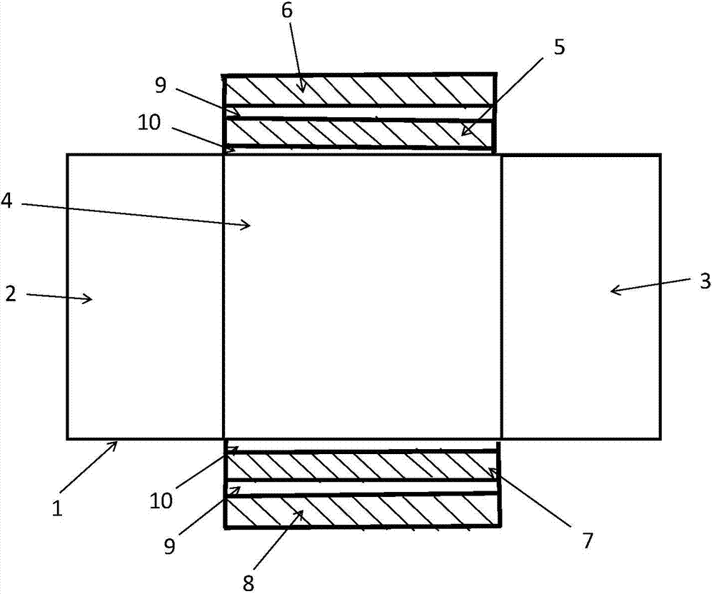
[0030] In the following specific embodiments of the present invention, please refer to figure 1 , figure 1 It is a structural schematic diagram of a dual-bit flash memory according to an embodiment of the present invention. Such as figure 1 As shown, the dual-bit flash memory memory of the present invention includes a semiconductor substrate 1, wh...


PUM


Abstract

The invention discloses a double-bit flash memory, which comprises a P-type substrate, a first floating gate, a second floating gate, a first control gate and a second control gate, wherein the P-type substrate comprises a source terminal and a drain terminal; the first floating gate, the second floating gate, the first control gate and the second control gate are sequentially located at the upper side and the lower side of the substrate; the first floating gate and the second floating gate are N-type doped polycrystalline silicon; the second control gate is made of P-type polycrystalline silicon; the second control gate is made of N-type polycrystalline silicon; in a programming process, positive drain terminal voltage is exerted on the drain terminal; the source terminal is grounded; the state of electrons stored in the corresponding floating gate is defined to be '1'; if the '1' state is programmed on any control gate, positive grid voltage is exerted on the corresponding control grid, so that an electronic inversion layer is generated on the groove of the substrate; under the accelerating action of the drain terminal voltage, groove electrons obtain enough energy and jump across a potential barrier between a grid oxidation layer and substrate silicon to become hot electrons; the hot electrons are injected into the floating gates to finish programming under the action of the grid voltage. According to the double-bit flash memory, the storage capacity per unit area of a floating gate flash memory is expanded, so that the dimension of the floating gate flash memory can be reduced.

Description

technical field [0001] The present invention relates to the technical field of semiconductors, more specifically, to a double-gate double-bit flash memory and programming, erasing and reading methods thereof. Background technique [0002] In semiconductor storage devices, flash memory (Flash Memory) is a long-life non-volatile (that is, it can still maintain stored data information in the case of power failure) memory. Flash memory is a variant of electronically erasable read-only memory (EEPROM). Because it can still save data when power is turned off, it can usually be used to save setting information, such as in the BIOS (basic program) of a computer, PDA (personal digital assistant) , Save data in digital cameras, etc. The characteristic of flash memory is that it can perform fast erasing operation in block (sector) unit. The writing operation of the flash memory must be carried out in the blank area. If the target area already has data, it must be erased before writin...

Claims


Application Information

Patent Timeline
Patent Type & Authority Applications(China)
IPC IPC(8): G11C16/10G11C16/14G11C16/26
CPCG11C11/5628G11C11/5635G11C11/5642G11C16/0441G11C2211/5612H01L29/42332H01L29/66825H01L29/7887H01L29/42328
Inventor 顾经纶阎江
Owner SHANGHAI HUALI MICROELECTRONICS CORP
Why Eureka
Try Eureka