Grating groove manufacturing method for silicon carbide device

A manufacturing method and technology of silicon carbide, applied in semiconductor/solid-state device manufacturing, semiconductor devices, electrical components, etc., can solve the problems of reducing device stability and reliability, electric field concentration, etc., to improve breakdown performance and reliability, The effect of reducing the electric field concentration effect

Inactive Publication Date: 2015-06-24
UNIV OF ELECTRONICS SCI & TECH OF CHINA
View PDF5 Cites 3 Cited by
  • Summary
  • Abstract
  • Description
  • Claims
  • Application Information

AI Technical Summary

Problems solved by technology

The existence of micro-grooves will lead to the concentration of the electric field at the bottom of the gate groove of the device, reducing the stability and reliability of the device

Method used


Image

  • Grating groove manufacturing method for silicon carbide device
  • Grating groove manufacturing method for silicon carbide device
  • Grating groove manufacturing method for silicon carbide device

Examples


Embodiment Construction

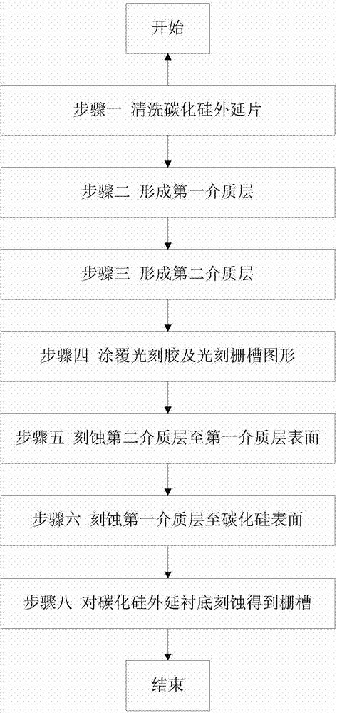
[0050] The present invention is described in detail below in conjunction with accompanying drawing

[0051] Such as Figure 10 As shown, it is a flow chart of the gate groove manufacturing method of the silicon carbide UMOS device of the present invention; as Figure 11 to Figure 18 Shown is a schematic diagram of the structure of each step of the method for fabricating a gate groove of a silicon carbide UMOS device according to the present invention. The method for forming the gate trench in the embodiment of the present invention includes the following steps:

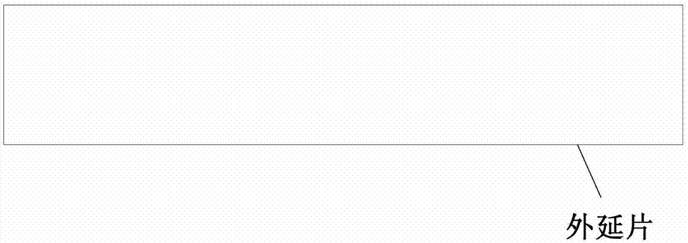
[0052] Step 1: If Figure 11 As shown, clean the silicon carbide epitaxial wafer;

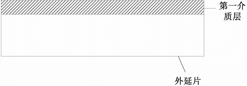
[0053] Step 2: If Figure 12 As shown, a first dielectric layer is formed on the silicon carbide epitaxial wafer;

[0054] Step 3: If Figure 13 As shown, a second dielectric layer is formed on the first dielectric layer, and the composition material of the second dielectric layer is different from the composition material of the f...


PUM


Abstract

The invention relates to a semiconductor manufacturing technology, in particular to a grating groove manufacturing method for silicon carbide UMOS device. According to the grating groove manufacturing method for the silicon carbide device, mainly, a dielectric layer on a silicon carbide epitaxial wafer is etched according to a grating groove area window, part of the dielectric layer on the upper surface of silicon carbide is reserved during etching, and then the part of the dielectric layer is corroded through a corrosion technology, so that the area where the dielectric layer makes contact with the silicon carbide epitaxial wafer forms a smooth arc, and a silicon carbide grating groove structure with a steep side wall, without a micro groove and with smooth bottom feet is formed on the silicon carbide epitaxial wafer after etching. The method has the advantages that the silicon carbide grating groove structure with the steep side wall, without the micro groove and with the smooth bottom feet is obtained, the electric field concentration effect at the bottom of a groove grate is reduced, and breakdown property and reliability of the device are improved. The method is particularly applicable to silicon carbide grating groove structure manufacturing.

Description

technical field [0001] The invention relates to a semiconductor manufacturing process, in particular to a method for manufacturing a gate groove of a silicon carbide UMOS device. Background technique [0002] Silicon carbide material has excellent physical and electrical properties. With its unique advantages such as large band gap, high critical breakdown electric field, high thermal conductivity and high saturation drift speed, it has become a high-voltage, high-power, high-temperature-resistant, high-frequency, anti- It is an ideal semiconductor material for irradiation devices and has broad application prospects in military and civil affairs. Power electronic devices made of silicon carbide materials have become one of the hot devices and frontier research fields in the field of semiconductors. [0003] Silicon carbide materials have high hardness and stable chemical properties, and it is difficult to form various structures through wet etching. At present, only dry etc...

Claims


Application Information

Patent Timeline
Patent Type & Authority Applications(China)
IPC IPC(8): H01L21/336
CPCH01L21/28H01L29/66068
Inventor 邓小川萧寒户金豹申华军李妍月唐亚超甘志梁坤元张波
Owner UNIV OF ELECTRONICS SCI & TECH OF CHINA
Why Eureka
Try Eureka