
Optical Semiconductor Device

An optical semiconductor and device technology, applied in optics, nonlinear optics, instruments, etc., can solve problems such as higher modulation efficiency and narrower wavelength bandwidth.

Inactive Publication Date: 2015-07-01
FUJITSU LTD
View PDF6 Cites 3 Cited by
  • Summary
  • Abstract
  • Description
  • Claims
  • Application Information

AI Technical Summary

Problems solved by technology

[0005] However, the ring modulator has a problem of narrowing the wavelength bandwidth while making the modulation efficiency high

Method used


Image

  • Optical Semiconductor Device
  • Optical Semiconductor Device
  • Optical Semiconductor Device

Examples


no. 1 example

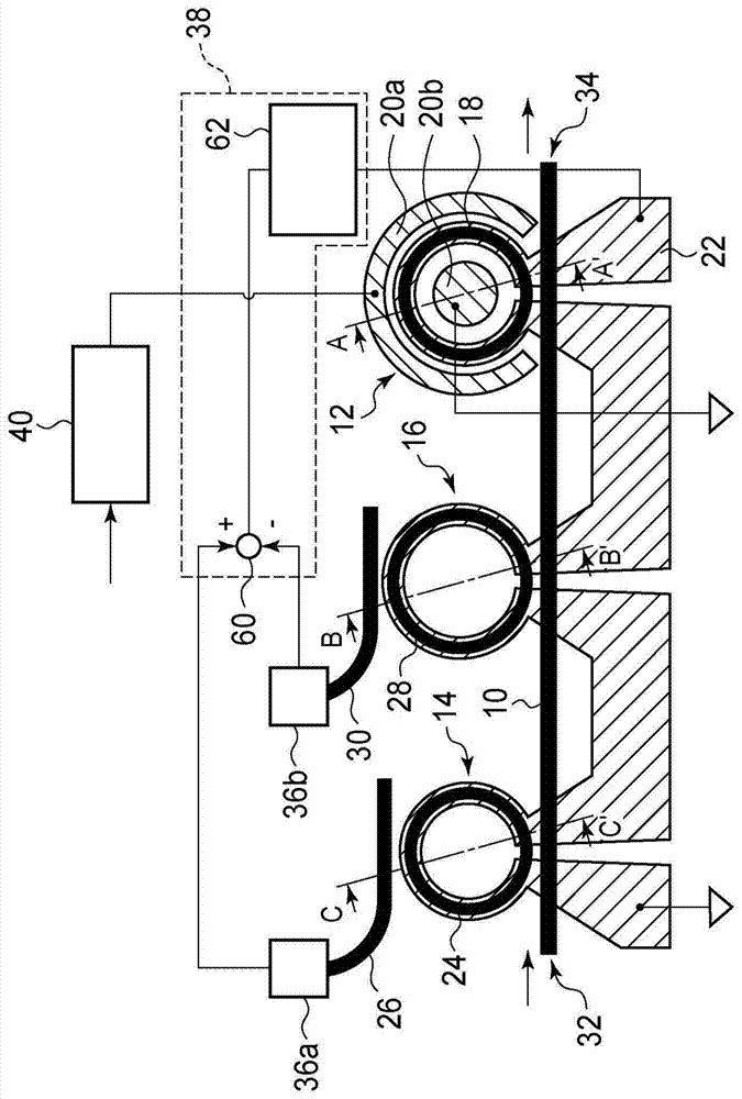
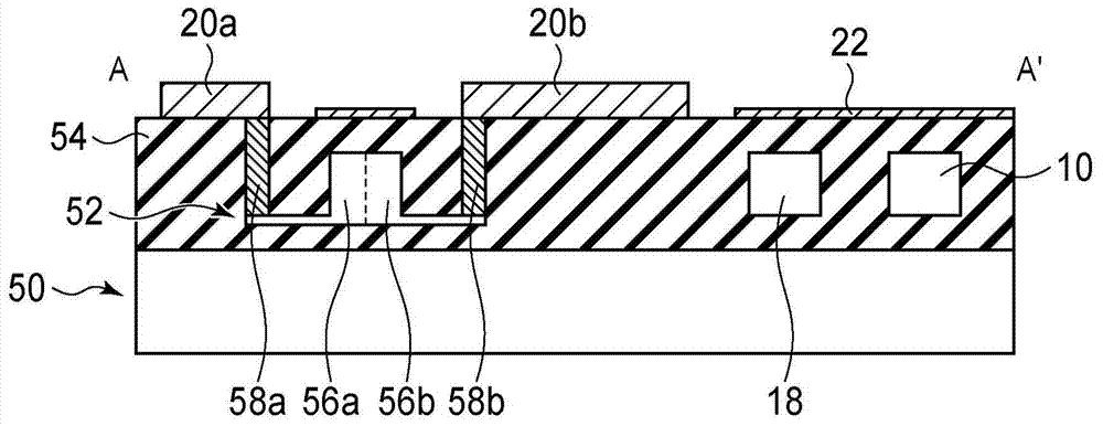
[0028] will refer to Figure 1 to Figure 14 An optical semiconductor device according to the first embodiment is described.

[0029] figure 1 is a schematic diagram showing the optical semiconductor device according to the present embodiment. Figure 2 to Figure 4 is a cross-sectional view showing the optical semiconductor according to the present embodiment. Figure 5 , Figure 6 , Figure 10 as well as Figure 11 is a graph showing the relationship between the modulated light output power of an optical resonator and the wavelength of input light. Figure 7 and Figure 8 is a graph showing the relationship between the monitored current and the wavelength of input light. Figure 9 and Figure 13 is a schematic diagram showing an optical semiconductor device according to a reference example. Figure 12 is a graph showing the relationship between the monitored light power and the wavelength of the input light. Figure 14 is a graph showing the relationship between the ...

no. 2 example

[0084] will refer to Figure 15 An optical semiconductor device according to a second embodiment is described. Denote this embodiment with the same reference numerals according to Figure 1 to Figure 14 The same components are shown as the optical semiconductor device of the first embodiment so as not to repeat or simplify the description.

[0085] Figure 15 is a schematic diagram showing the optical semiconductor device according to the present embodiment.

[0086] The optical semiconductor device according to the present embodiment is the same as the optical semiconductor device according to the first embodiment except for the planar configuration of the ring waveguide.

[0087] That is, the optical semiconductor device according to the present embodiment includes ring waveguides 18a, 24a, 28a instead of ring waveguides 18, 24, 28 each having four linear portions and four arcuate portions. Composite Structure.

[0088] The arc of the ring waveguides 18a, 24a, 28a is a ...

no. 3 example

[0094] will refer to Figure 16 An optical semiconductor device according to a third embodiment is described. Denote this embodiment with the same reference numerals according to Figure 1 to Figure 15 The same components of the optical semiconductor devices of the first and second embodiments are shown so as not to repeat or simplify the description.

[0095] Figure 16is a schematic sectional view showing the optical semiconductor device according to the present embodiment.

[0096] The optical semiconductor device according to the present embodiment is the same as the optical semiconductor device according to the first embodiment except that the second optical resonator 14 and the third optical resonator 16 are disposed opposite to each other.

[0097] With the second optical resonator 14 and the third optical resonator 16 disposed oppositely, the optical semiconductor device can operate in the same manner as the optical semiconductor device according to the first embodi...


PUM


Abstract

An optical semiconductor device includes a waveguide that an input light to be inputted, a ring modulator optically coupled with the waveguide, a first ring resonator optically coupled with the waveguide and having an optical path length smaller than an optical path length of the ring modulator, a second ring resonator optically coupled with the first waveguide and having an optical path length larger than the optical path length of the ring modulator, a heater arranged adjacent to the ring modulator, the first ring resonator and the second ring resonator, a first photodetector monitoring a light power in the first ring resonator, a second photodetector monitoring a light power in the second ring resonator, and a controller controlling the heater so that a resonance wavelength of the ring modulator agrees with a wavelength of the input light, based on signals detected by the first and second photodetectors.

Description

[0001] This application is a divisional application of the invention patent application with the application number 201210272727.6, the invention name is "Optical Semiconductor Device", and the application date is August 2, 2012. technical field [0002] Embodiments discussed herein relate to optical semiconductor devices. Background technique [0003] Implementing optics on silicon is critical for miniaturized, high-capacity, and low-power optical transmitters and optical receivers. Optical devices on silicon can use optical waveguides with large refractive index differences, which is more conducive to miniaturization than optical devices on other materials, which facilitates integration with other electronic circuits, resulting in many optical transmitters and optical receivers can be integrated on one chip. In optics, especially the properties of the modulator affect the power consumption and size of the optical transmitter and optical receiver. In particular, a ring mo...

Claims


Application Information

Patent Timeline
Patent Type & Authority Applications(China)
IPC IPC(8): G02F1/01
CPCG02F1/0147G02F1/0115G02F2203/15
Inventor 秋山知之
Owner FUJITSU LTD
Learn More