Multistage sweeping type silicon slice texturing and processing device and control method thereof

A technology of a processing device and a control method, which is applied in the manufacturing of final products, sustainable manufacturing/processing, discharge tubes, etc., can solve the problem that the damage removal layer and texturing of silicon wafers cannot be completed at one time, the on-line processing of industrial lines cannot be realized, and the drying process is hindered. Solving problems such as the industrialization process of etching method, to achieve the effect of fast and efficient silicon wafer processing, reducing adhesion by-products, and solving industrialization problems

Active Publication Date: 2015-07-01
江苏盎华光伏工程技术研究中心有限公司
View PDF3 Cites 5 Cited by
  • Summary
  • Abstract
  • Description
  • Claims
  • Application Information

AI Technical Summary

Problems solved by technology

However, there are still some problems in the dry etching of silicon wafers, such as: the thick surface lattice damage layer caused by the bombardment of high-energy particles, the slow etching rate of silicon wafers by a single plasma source, and the removal of damaged layers and texturing of silicon wafers cannot be completed at one time , cannot realize the on-line processing of the industrial line, and needs to cooperate with acid and alkali liquid pretreatment and post-treatment, etc., which hinders the industrialization process of dry etching

Method used


Image

  • Multistage sweeping type silicon slice texturing and processing device and control method thereof
  • Multistage sweeping type silicon slice texturing and processing device and control method thereof

Examples


Embodiment Construction

[0026] The present invention will be further described below in conjunction with the accompanying drawings and embodiments.

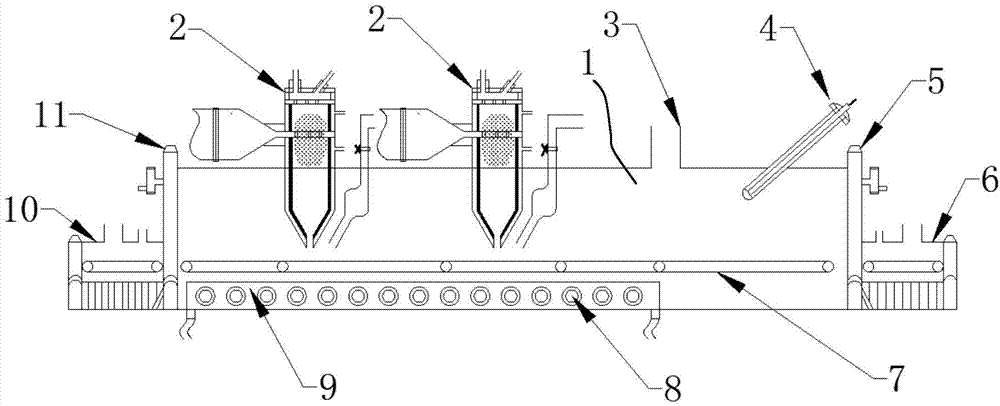
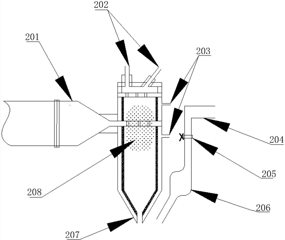
[0027] figure 1 It is a structural schematic diagram of the multi-stage purging type silicon wafer texturing treatment device of the present invention.

[0028] See figure 1 , the multi-stage purging type silicon wafer texture processing device provided by the present invention includes a reaction chamber 1, and a silicon wafer movement stage 7 is arranged in the reaction chamber 1, wherein, on the reaction chamber 1, at least There are two plasma downstream purging processing units 2, a front buffer chamber 10 and a front gate valve 11 are provided at the entrance of the reaction chamber 1, and a rear buffer chamber is provided at the exit of the reaction chamber 1. chamber 6 and rear gate valve 5, the reaction chamber 1 is provided with a reaction chamber vacuum outlet 3 near the rear buffer chamber 6, and a constant temperature radiation block 9 is...


PUM


Abstract

The invention discloses a multistage sweeping type silicon slice texturing and processing device and a control method thereof. The multistage sweeping type silicon slice texturing and processing device comprises a reaction chamber. A silicon slice moving carrier is arranged in the reaction chamber. At least two plasma downstream sweeping type processing units are arranged on the reaction chamber. A front buffer chamber and a front sluice valve are arranged at an inlet of the reaction chamber. A rear buffer chamber and a rear sluice valve are arranged at an outlet of the reaction chamber. A reaction chamber vacuum suction port is arranged at a position, close to the rear buffer chamber, on the reaction chamber. A constant-temperature radiation block is arranged below the silicon slice moving carrier. The multistage sweeping type silicon slice texturing and the processing device and a control method thereof have the advantages that the multistage sweeping type silicon slice processing units are adopted, independent working gas flow proportion and etching time can be adopted conveniently, and a rapid and efficient silicon slice processing process is achieved; etching speed is increased by the silicon slice moving carrier and the constant-temperature radiation block, so that online continuous processing is achieved, and silicon slice texturing effect is improved.

Description

technical field [0001] The invention relates to a silicon chip processing device and a control method thereof, in particular to a multi-stage purging type silicon chip texture processing device and a control method thereof. Background technique [0002] Silicon solar cell power generation has been considered to be one of the mainstream technologies for future green energy. The market share of silicon solar cells far exceeds that of other types of solar cells, with a market share of more than 90%. With various high-efficiency silicon solar cell processes entering industrial production, the photoelectric conversion efficiency of silicon solar cells has been continuously improved in recent years. High-efficiency polycrystalline silicon solar cells have an efficiency of about 19%, and high-efficiency monocrystalline silicon solar cells have an efficiency of about 21%. [0003] In all high-efficiency silicon solar cell processes, realizing the texture effect with low reflectivit...

Claims


Application Information

Patent Timeline
Patent Type & Authority Applications(China)
IPC IPC(8): H01L31/18H01J37/32
CPCH01J37/32H01L31/18Y02P70/50
Inventor 高文秀李帅赵百通
Owner 江苏盎华光伏工程技术研究中心有限公司
Why Eureka
Try Eureka