Cutting method of wafer grade white-light LED chip

A technology of LED chip and cutting method, applied in electrical components, circuits, semiconductor devices, etc., can solve the problems of chip fluorescent glue damage, substrate cracking, affecting product yield and reliability, etc., to improve production yield, avoid broken effect

Inactive Publication Date: 2015-07-01
LATTICE POWER (JIANGXI) CORP
View PDF10 Cites 18 Cited by
  • Summary
  • Abstract
  • Description
  • Claims
  • Application Information

AI Technical Summary

Problems solved by technology

If the wafer-level white LED chip is cut with a blade, the fluorescent adhesive layer will stick to the blade, causing a series of defects such as damage to the fluorescent adhesive on the chip surface, rolling up of the metal on the substrate, and cracking of the substrate, which will affect the quality of the product. Yield and Reliability
Although laser cutting can avoid the above problems, the laser will burn the side of the fluorescent adhesive layer black, causing light absorption and reducing the brightness of the white LED chip

Method used


Image

  • Cutting method of wafer grade white-light LED chip
  • Cutting method of wafer grade white-light LED chip
  • Cutting method of wafer grade white-light LED chip

Examples


Embodiment Construction

[0013] In order to make the technical problems, technical solutions and beneficial effects solved by the present invention clearer, the present invention will be further described in detail below in conjunction with the embodiments.

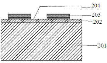
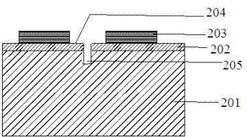
[0014] As shown in FIG. 2, a cutting method of a wafer-level white light LED chip includes preparing a GaN wafer with a vertical structure on a silicon substrate 201, such as Figure 2a , 202 in the figure is a conductive reflective composite metal layer, and the GaN LED 203 is separated by the scribe line 204; the 355nm ultraviolet laser emitted by the laser is focused to the middle position of the upper surface groove scribe line 204 of the silicon substrate 201, forming a 30 ±5 μm, groove 205 with a width of 10±2 μm, such as Figure 2b ; Coating a 30 μm thick fluorescent adhesive layer 206 on the wafer, making it distributed on the entire chip surface, and then baking and curing, as Figure 2c ; Mechanically grind and thin the silicon substra...


PUM


Abstract

The invention provides a cutting method of a wafer grade white-light LED chip. The method comprises the steps of preparing a vertical structural GaNLED wafer chip by the substrate transfer process; cutting a cutting channel in the front surface of the wafer through laser to form a concave groove; coating a fluorescent coating on the wafer chip; baking and solidifying; thinning the rear surface of the wafer chip; evaporating a back metal layer; performing back cutting for the wafer chip through a blade, wherein the cutting position is corresponding to the concave groove in the front surface; splitting along the concave groove in the wafer ship to obtain single white-light LED chip. With the adoption of the method, the wafer grade white-light LED chip can be smoothly separated without damaging the fluorescent glue layer on the surface of the LED chip, so that the phenomena of breaking and cracking in the traditional cutting process can be avoided, and the yield of white-light LED can be increased.

Description

technical field [0001] The invention relates to the field of production and preparation of light-emitting diodes. More specifically, the present invention relates to a cutting method of wafer-level white light LED chips. Background technique [0002] Usually, the manufacturing method of realizing white light LED is to fix a single GaN blue light chip on the bracket by packaging technology, and obtain white light LED after wiring, dotting fluorescent glue or spraying fluorescent glue. The process of producing white light LEDs is complicated, and the light output efficiency of the chip is low, and because the consistency of the thickness of the fluorescent glue on the chip surface is difficult to control, the light emission of LED products is uneven, which adds difficulties to the secondary optical design. [0003] In order to solve the problems in conventional methods, a method for preparing wafer-level white LED chips has emerged. The method is obtained by using a fluoresc...

Claims


Application Information

Patent Timeline
Patent Type & Authority Applications(China)
IPC IPC(8): H01L33/00H01L21/78
CPCH01L33/005H01L21/78H01L2933/0008
Inventor 封波刘乐功
Owner LATTICE POWER (JIANGXI) CORP
Why Eureka
Try Eureka